From Verilog to GDSII
The generated Verilog code can be used through a semi-custom design flow to generate the layout.
Because of the commercial nature of the semi-custom design tools we are using, we cannot share the different scripts that we are using. However, we can show the results to serve as a proof-of-concept and encourage research through it.
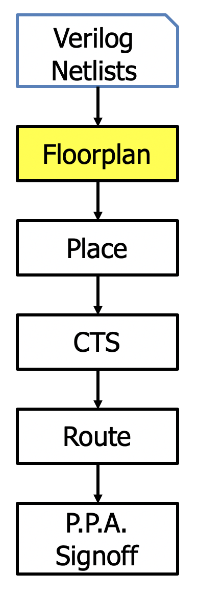
Layout_Diagram shows the different steps involved in realizing the layout for any design. CTS stands for Clock Tree Synthesis, and PPA stands for Power-Performance-Area. First, we create the floorplan with the different tiles involved in the FPGA, i.e., the CLBs and place them. Then the clock tree is generated. Finally, the design is routed, and the PPA signoff is realized. Coupled with FPGA-SPICE, we get silicon level analysis on the design.
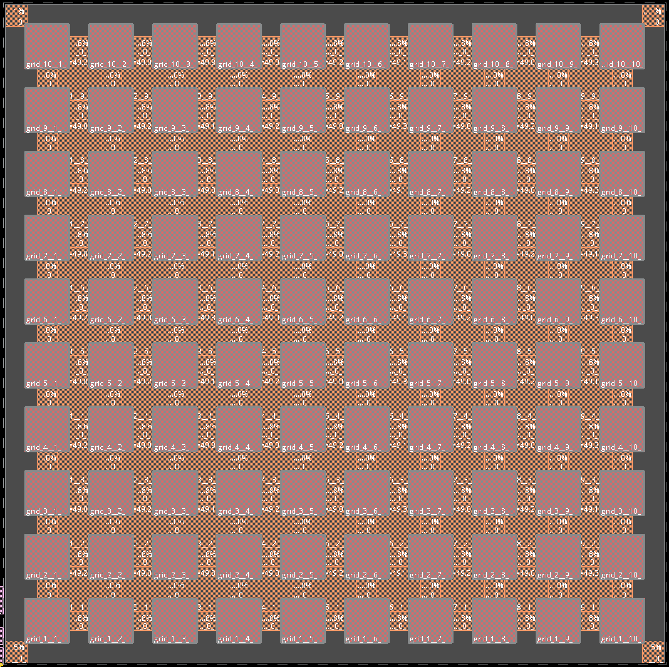
In Layout_Floorplan, we show the result we get from the floorplanning we get through Cadence Innovus.