Circuit Library
Circuit design is a dominant factor in Power, Performance, Area (P.P.A.) of FPGA fabrics. Upon practical applications, the hardware engineers may select various circuits to implement their FPGA fabrics. For instance, a ultra-low-power FPGA may be built with ulta-low-power circuit cells while a high-performance FPGA may use absolutely different circuit cells. OpenFPGA provide enriched XML syntax for users to highly customize their circuits in FPGA fabric.
In the XML file, users can define a library of circuits, each of which corresponds to a primitive module required in the FPGA architecture. Users can specify if the Verilog/SPICE netlist of the module is either auto-generated by OpenFPGA or provided by themselves. As such, OpenFPGA can support any circuit design, leading to high flexibility in building FPGA fabrics.
In principle, a circuit library consists of a number of <circuit_model>, each of which correspond to a circuit design.
OpenFPGA supports a wide range of circuit designs.
The <circuit_model> could be as small as a cornerstone cell, such as inverter, buffer etc., or as large as a hardware IP, such as Block RAM.
<circuit_library>
  <circuit_model type="<string>" name="<string>">
    <!-- Detailed circuit-level design parameters -->
  </circuit_model>
  <!-- More circuit models -->
</circuit_library>
Currently, OpenFPGA supports the following categories of circuits:
inverters/buffers
pass-gate logic, including transmission gates and pass transistors
standard cell logic gates, including AND, OR and MUX2
metal wires
multiplexers
flip-flops
Look-Up Tables, including single-output and multi-output fracturable LUTs
Statis Random Access Memory (SRAM)
scan-chain flip-flops
I/O pad
hardware IPs
Circuit Model
As OpenFPGA supports many types of circuit models and their circuit-level implementation could be really different, each type of circuit model has special syntax to customize their designs. However, most circuit models share the common generality in XML language. Here, we focus these common syntax and we will detail special syntax in Circuit model examples
<circuit_model type="<string>" name="<string>" prefix="<string>" is_default="<bool>" spice_netlist="<string>" verilog_netlist="<string>" dump_structural_verilog="<bool>">
  <design_technology type="<string>"/>
  <input_buffer exist="<string>" circuit_model_name="<string>"/>
  <output_buffer exist="<string>" circuit_model_name="<string>"/>
  <pass_gate_logic type="<string>" circuit_model_name="<string>"/>
  <last_stage_pass_gate_logic type="<string>" circuit_model_name="<string>"/>
  <port type="<string>" prefix="<string>" lib_name="<string>" size="<int>" default_val="<int>" circuit_model_name="<string>" mode_select="<bool>" is_global="<bool>" is_set="<bool>" is_reset="<bool>" is_config_enable="<bool>"/>
  <!-- more ports -->
</circuit_model>
- <circuit_model type="<string>" name="<string>" prefix="<string>" is_default="<bool>"
- spice_netlist="<string>" verilog_netlist="<string>" dump_structural_verilog="<bool>">
Specify the general attributes for a circuit model
type="inv_buf|pass_gate|gate|mux|wire|chan_wire|sram|lut|ff|ccff|hard_logic|iopad"Specify the type of circuit model. For the circuit models in the type of mux/wire/chan_wire/lut, FPGA-Verilog/SPICE can auto-generate Verilog/SPICE netlists. For the rest, FPGA-Verilog/SPICE requires a user-defined Verilog/SPICE netlist.name="<string>"Specify the name of this circuit model. The name should be unique and will be used to create the Verilog/SPICE module in Verilog/SPICE netlists. Note that for a customized Verilog/SPICE netlist, the name defined here MUST be the name in the customized Verilog/SPICE netlist. FPGA-Verilog/SPICE will check if the given name is conflicted with any reserved words.prefix="<string>"Specify the name of the<circuit_model>to shown in the auto-generated Verilog/SPICE netlists. The prefix can be the same as the name defined above. And again, the prefix should be uniqueis_default="true|false"Specify this circuit model is the default one for those in the same types. If a primitive module in VPR architecture is not linked to any circuit model by users, FPGA-Verilog/SPICE will find the default circuit model defined in the same type.spice_netlist="<string>"Specify the path and file name of a customized SPICE netlist. For some modules such as SRAMs, FFs, I/O pads, FPGA-SPICE does not support auto-generation of the transistor-level sub-circuits because their circuit design is highly dependent on the technology nodes. These circuit designs should be specified by users. For the other modules that can be auto-generated by FPGA-SPICE, the user can also define a custom netlist.verilog_netlist="<string>"Specify the path and file name of a customized Verilog netlist. For some modules such as SRAMs, FFs, I/O pads, FPGA-Verilog does not support auto-generation of the transistor-level sub-circuits because their circuit design is highly dependent on the technology nodes. These circuit designs should be specified by users. For the other modules that can be auto-generated by FPGA-Verilog, the user can also define a custom netlist.dump_structural_verilog="true|false"When the value of this keyword is set to be true, Verilog generator will output gate-level netlists of this module, instead of behavior-level. Gate-level netlists bring more opportunities in layout-level optimization while behavior-level is more suitable for high-speed formal verification and easier in debugging with HDL simulators.
Warning
prefix may be deprecated soon
Warning
Multiplexers cannot be user-defined.
Warning
For a circuit model type, only one circuit model is allowed to be set as default. If there is only one circuit model defined in a type, it will be considered as the default automatically.
Note
If <spice_netlist> or <verilog_netlist> are not specified, FPGA-Verilog/SPICE auto-generates the Verilog/SPICE netlists for multiplexers, wires, and LUTs.
Note
The user-defined netlists, such as LUTs, the decoding methodology should comply with the auto-generated LUTs!!!
Design Technology
- <design_technology type="string"/>
Specify the design technology applied to a
<circuit_model>type="cmos|rram"Specify the type of design technology of the<circuit_model>. Currently, OpenFPGA supports CMOS and RRAM technology for circuit models. CMOS technology can be applied to any types of<circuit_model>, while RRAM technology is only applicable to multiplexers and SRAMs
Note
Each <circuit_model> may have different technologies
Device Technology
- <device_technology device_model_name="<string>"/>
Specify the technology binding between a circuit model and a device model which is defined in the technology library (see details in Technology library).
device_model_name="<string>"Specify the name of device model that the circuit design will use. The device model must be a valid one in the technology library.
Note
Technology binding is only required for primitive circuit models, which are inverters, buffers, logic gates, pass gate logic, and is mandatory only when SPICE netlist generation is required.
Input and Output Buffers
- <input_buffer exist="<string>" circuit_model_name="<string>"/>
exist="true|false"Define the existence of the input buffer. Note that the existence is valid for all the inputs.circuit_model_name="<string>"Specify the name of circuit model which is used to implement input buffer, the type of specified circuit model should beinv_buf.
- <output_buffer exist="<string>" circuit_model_name="<string>"/>
exist="true|false"Define the existence of the output buffer. Note that the existence is valid for all the outputs. Note that if users want only part of the inputs (or outputs) to be buffered, this is not supported here. A solution can be building a user-defined Verilog/SPICE netlist.circuit_model_name="<string>"Specify the name of circuit model which is used to implement the output buffer, the type of specified circuit model should beinv_buf.
Note
If users want only part of the inputs (or outputs) to be buffered, this is not supported here. A solution can be building a user-defined Verilog/SPICE netlist.
Pass Gate Logic
Note
pass-gate logic are used in building multiplexers and LUTs.
- <pass_gate_logic circuit_model_name="<string>"/>
circuit_model_name="<string>"Specify the name of the circuit model which is used to implement pass-gate logic, the type of specified circuit model should bepass_gate.
- <last_stage_pass_gate_logic circuit_model_name="<string>"/>
circuit_model_name="<string>"Specify the name of the circuit model which is used to implement the pass-gate logic at last stage of multiplexer, the type of specified circuit model should bepass_gate. The type of the pass-gate logic circuit model must be a standard cell MUX2!
Circuit Port
A circuit model may consist of a number of ports. The port list is mandatory in any circuit_model and must be consistent to any user-defined netlists.
- <port type="<string>" prefix="<string>" lib_name="<string>" size="<int>"
- default_val="<int>" circuit_model_name="<string>" mode_select="<bool>"
- is_global="<bool>" is_set="<bool>" is_reset="<bool>"
- is_config_enable="<bool>" is_io="<bool>" is_data_io="<bool>"/>
Define the attributes for a port of a circuit model.
type="input|output|sram|clock"Specify the type of the port, i.e., the directionality and usage. For programmable modules, such as multiplexers and LUTs, SRAM ports MUST be defined. For registers, such as FFs and memory banks, clock ports MUST be defined.Note
sramandclockports are considered as inputs in terms of directionalityprefix="<string>"the name of the port to appear in the autogenerated netlists. Each port will be shown as<prefix>[i]in Verilog/SPICE netlists.Note
if the circuit model is binded to a
pb_typein VPR architecture,prefixmust match the port name defined inpb_typelib_name="<string>"the name of the port defined in standard cells or customized cells. If not specified, this attribute will be the same asprefix.Note
if the circuit model comes from a standard cell library, using
lib_nameis recommended. This is because - the port names defined inpb_typeare very diffrerent from the standard cells - the port sequence is very differentsize="<int>"bandwidth of the port. MUST be larger than zero.default_val="<int>"Specify default logic value for a port, which is used as the initial logic value of this port in testbench generation. Can be either 0 or 1. We assume each pin of this port has the same default value.circuit_model_name="<string>"Specify the name of the circuit model which is connected to this port.Note
circuit_model_nameis only valid when the type of this port issram.is_io="true|false"Specify if this port should be treated as an I/O port of an FPGA fabric. When this is enabled, this port of each circuit model instanciated in FPGA will be added as an I/O of an FPGA.Note
global
outputports must beioportsis_data_io="true|false"Specify if this port should be treated as a mappable FPGA I/O port for users’ implementation. When this is enabled, I/Os of user’s implementation, e.g.,.inputand.outputin.blifnetlist, can be mapped to the port through VPR.Note
Any I/O model must have at least 1 port that is defined as data I/O!
mode_select="true|false"Specify if this port controls the mode switching in a configurable logic block. This is due to that a configurable logic block can operate in different modes, which is controlled by SRAM bits.Note
mode_selectis only valid when the type of this port issram.is_global="true|false"can be eithertrueorfalse. Specify if this port is a global port, which will be routed globally.Note
For input ports, when multiple global input ports are defined with the same name, by default, these global ports will be short-wired together. When
iois turned on for this port, these global ports will be independent in the FPGA fabric.Note
For output ports, the global ports will be independent in the FPGA fabric
is_set="true|false"Specify if this port controls a set signal. All the set ports are connected to global set voltage stimuli in testbenches.is_reset="true|false"Specify if this port controls a reset signal. All the reset ports are connected to a global reset voltage stimuli in testbenches.is_config_enable="true|false"Specify if this port controls a configuration-enable signal. Only valid whenis_globalistrue. This port is only enabled during FPGA configuration, and always disabled during FPGA operation. All theconfig_enableports are connected to global configuration-enable voltage stimuli in testbenches.
Note
This attribute is used by testbench generators (see Testbench)
In full testbench,
There is a
config_donesignal, which stay at logic0during bitstream loading phase, and is pulled up to logic1during operating phaseWhen
default_value="0", the port will be wired to aconfig_donesignal.When
default_value="1", the port will be wired to an invertedconfig_donesignal.
In preconfigured wrapper, the port will be set to the inversion of
default_value, as the preconfigured testbenches consider operating phase only.
Note
is_set, is_reset and is_config_enable are only valid when is_global is true.
Note
Different types of circuit_model have different XML syntax, with which users can highly customize their circuit topologies. See refer to examples of :ref:circuit_model_example for more details.
Note
Note that we have a list of reserved port names, which indicate the usage of these ports when building FPGA fabrics. Please do not use mem_out, mem_inv, bl, wl, blb, wlb, wlr, ccff_head and ccff_tail.
FPGA I/O Port
The circuit_model support not only highly customizable circuit-level modeling but also flexible I/O connection in the FPGA fabric.
Typically, circuit ports appear in the primitive modules of a FPGA fabric.
However, it is also very common that some circuit ports should be I/O of a FPGA fabric.
Using syntax is_global and is_io, users can freely define how these ports are connected as FPGA I/Os.
In principle, when is_global is set true, the port will appear as an FPGA I/O.
The syntax is_io is applicable when is_global is true.
When is_io is true, the port from different instances will be treated as independent I/Os.
When is_io is false, the port from different instances will be treated as the same I/Os, which are short-wired.
To beef up, the following examples will explain how to use is_global and is_io to achieve different types of connections to FPGA I/Os.
- Global short-wired inputs
<port type="input" is_global="true" is_io="false"/>
The global inputs are short wired across different instances. These inputs are widely seen in FPGAs, such as clock ports, which are shared between sequential elements.
Fig. 37 shows an example on how the global inputs are wired inside FPGA fabric.
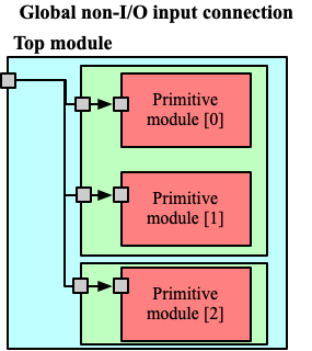
Fig. 37 Short-wired global inputs as an FPGA I/O
- Global short-wired inouts
<port type="inout" is_global="true" is_io="false"/>
The global inouts are short wired across different instances.
Fig. 38 shows an example on how the global inouts are wired inside FPGA fabric.
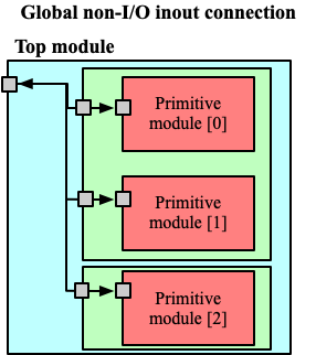
Fig. 38 Short-wired global inouts as an FPGA I/O
- General-purpose inputs
<port type="input" is_global="true" is_io="true"/>
The general-purpose inputs are independent wired from different instances to separated FPGA I/Os. For example, power-gating signals can be applied to each tile of a FPGA.
Fig. 39 shows an example on how the general-purpose inputs are wired inside FPGA fabric.
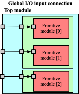
Fig. 39 General-purpose inputs as separated FPGA I/Os
- General-purpose I/O
<port type="inout" is_global="true" is_io="true"/>
The general-purpose I/O are independent wired from different instances to separated FPGA I/Os. In practice, inout of GPIO cell is typically wired like this.
Fig. 39 shows an example on how the general-purpose inouts are wired inside FPGA fabric.
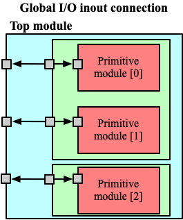
Fig. 40 General-purpose inouts as separated FPGA I/Os
- General-purpose outputs
<port type="output" is_global="true" is_io="true"/>
The general-purpose outputs are independent wired from different instances to separated FPGA outputs. In practice, these outputs are typically spypads to probe internal signals of a FPGA.
Fig. 41 shows an example on how the general-purpose outputs are wired inside FPGA fabric.
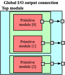
Fig. 41 General-purpose outputs as separated FPGA I/Os
Warning
The general-purpose inputs/inouts/outputs are not applicable to routing multiplexer outputs