Build an FPGA fabric using Standard Cell Libraries
Introduction
- In this tutorial, we will
Showcase how to create an architecture description based on standard cells, using OpenFPGA’s circuit modeling language
Use Skywater’s Process Design Kit (PDK) cell library to create an OR Gate circuit model for OpenFPGA
Verify that the standard cell library file was correctly bound into the selected architecture file by looking at auto-generated OpenFPGA files and checking simulation waveforms in GTKWave
Through this example, we will show how to bind standard cell library files with OpenFPGA Architectures.
Note
We showcase the methodology by considering the open-source Skywater 130nm PDK so that users can easily reproduce the results.
Create and Verify the OpenFPGA Circuit Model
Note
In this tutorial, we focus on binding a 2-input OR gate from a standard cell library to a circuit model in OpenFPGA’s architecture description file. Note that the approach can be generalized to any circuit model.
For this tutorial, we start with an example where the HDL netlist of an 2-input OR gate that is auto-generated by OpenFPGA. After updating the architecture file, the auto-generated HDL netlist created by OpenFPGA will directly instantiate a standard cell from the open-source Skywater 130nm PDK library. To follow along, go to the root directory of OpenFPGA and enter:
python3 openfpga_flow/scripts/run_fpga_task.py fpga_verilog/adder/hard_adder --debug --show_thread_logs
This will run a prebuilt task with OpenFPGA cell libraries. When the task is finished, there will be many auto-generated files to look through. For this tutorial, we are interested in the luts.v and and2_formal.vcd files. The OR2 gate is used as a control circuit in the lut6 circuit model, and the and2_formal.vcd file will have the resulting waveforms from the simulation run by the task. To open the luts.v file, run the following command:
vi openfpga_flow/tasks/fpga_verilog/adder/hard_adder/latest/k6_frac_N10_tileable_adder_chain_40nm/and2/MIN_ROUTE_CHAN_WIDTH/SRC/sub_module/luts.v
Note
Users can find full details about netlist organization in our documentation: Fabric Netlists
The luts.v file represents a Look Up Table within the OpenFPGA architecture. The important lines of this file for the tutorial are highlighted below.
These lines show the instantiation of OpenFPGA’s OR2 cell library.
 //-------------------------------------------
 //   FPGA Synthesizable Verilog Netlist
 //   Description: Look-Up Tables
 //   Author: Xifan TANG
 //   Organization: University of Utah
 //   Date: Tue Mar 30 15:25:03 2021
 //-------------------------------------------
 //----- Time scale -----
 `timescale 1ns / 1ps

 //----- Default net type -----
 `default_nettype none

 // ----- Verilog module for frac_lut6 -----
 module frac_lut6(in,
                  sram,
                  sram_inv,
                  mode,
                  mode_inv,
                  lut4_out,
                  lut5_out,
                  lut6_out);
 //----- INPUT PORTS -----
 input [0:5] in;
 //----- INPUT PORTS -----
 input [0:63] sram;
 //----- INPUT PORTS -----
 input [0:63] sram_inv;
 //----- INPUT PORTS -----
 input [0:1] mode;
 //----- INPUT PORTS -----
 input [0:1] mode_inv;
 //----- OUTPUT PORTS -----
 output [0:3] lut4_out;
 //----- OUTPUT PORTS -----
 output [0:1] lut5_out;
 //----- OUTPUT PORTS -----
 output [0:0] lut6_out;

 //----- BEGIN wire-connection ports -----
 wire [0:5] in;
 wire [0:3] lut4_out;
 wire [0:1] lut5_out;
 wire [0:0] lut6_out;
 //----- END wire-connection ports -----


 //----- BEGIN Registered ports -----
 //----- END Registered ports -----


 wire [0:0] INVTX1_0_out;
 wire [0:0] INVTX1_1_out;
 wire [0:0] INVTX1_2_out;
 wire [0:0] INVTX1_3_out;
 wire [0:0] INVTX1_4_out;
 wire [0:0] INVTX1_5_out;
 wire [0:0] OR2_0_out;
 wire [0:0] OR2_1_out;
 wire [0:0] buf4_0_out;
 wire [0:0] buf4_1_out;
 wire [0:0] buf4_2_out;
 wire [0:0] buf4_3_out;
 wire [0:0] buf4_4_out;
 wire [0:0] buf4_5_out;

 // ----- BEGIN Local short connections -----
 // ----- END Local short connections -----
 // ----- BEGIN Local output short connections -----
 // ----- END Local output short connections -----

      OR2 OR2_0_ (
              .a(mode[0:0]),
              .b(in[4]),
              .out(OR2_0_out));

      OR2 OR2_1_ (
              .a(mode[1]),
              .b(in[5]),
              .out(OR2_1_out));

      INVTX1 INVTX1_0_ (
              .in(in[0:0]),
              .out(INVTX1_0_out));

      INVTX1 INVTX1_1_ (
              .in(in[1]),
              .out(INVTX1_1_out));

      INVTX1 INVTX1_2_ (
              .in(in[2]),
              .out(INVTX1_2_out));

      INVTX1 INVTX1_3_ (
              .in(in[3]),
              .out(INVTX1_3_out));

      INVTX1 INVTX1_4_ (
              .in(OR2_0_out),
              .out(INVTX1_4_out));

      INVTX1 INVTX1_5_ (
              .in(OR2_1_out),
              .out(INVTX1_5_out));

      buf4 buf4_0_ (
              .in(in[0:0]),
              .out(buf4_0_out));

      buf4 buf4_1_ (
              .in(in[1]),
              .out(buf4_1_out));

      buf4 buf4_2_ (
              .in(in[2]),
              .out(buf4_2_out));

      buf4 buf4_3_ (
              .in(in[3]),
              .out(buf4_3_out));

      buf4 buf4_4_ (
              .in(OR2_0_out),
              .out(buf4_4_out));

      buf4 buf4_5_ (
              .in(OR2_1_out),
              .out(buf4_5_out));

      frac_lut6_mux frac_lut6_mux_0_ (
              .in(sram[0:63]),
              .sram({buf4_0_out, buf4_1_out, buf4_2_out, buf4_3_out, buf4_4_out, buf4_5_out}),
              .sram_inv({INVTX1_0_out, INVTX1_1_out, INVTX1_2_out, INVTX1_3_out, INVTX1_4_out, INVTX1_5_out}),
              .lut4_out(lut4_out[0:3]),
              .lut5_out(lut5_out[0:1]),
              .lut6_out(lut6_out));

 endmodule
 // ----- END Verilog module for frac_lut6 -----

 //----- Default net type -----
 `default_nettype none
We will also need to look at the control’s simulation waveforms. Viewing the waveforms is done through GTKWave with the following command:
gtkwave openfpga_flow/tasks/fpga_verilog/adder/hard_adder/latest/k6_frac_N10_tileable_adder_chain_40nm/and2/MIN_ROUTE_CHAN_WIDTH/and2_formal.vcd &
The simulation waveforms should look similar to the following Fig. 8:
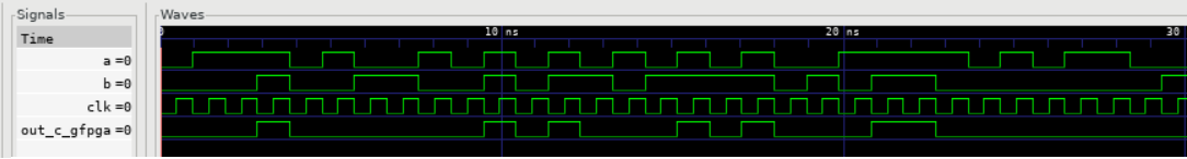
Fig. 8 Simulation Waveforms with OpenFPGA Circuit Model
Note
The waveform inputs do not need to exactly match because the testbench provides input in random intervals.
We have now finished creating the control and viewing the important sections for this tutorial. We can now incorporate Skywater’s cell library to create a new circuit model.
Clone Skywater PDK into OpenFPGA
We will be using the open-source Skywater PDK to create our circuit model. We start by cloning the Skywater PDK github repository into the OpenFPGA root directory. Run the following command in the root directory of OpenFPGA:
git clone https://github.com/google/skywater-pdk.git
Once the repository has been cloned, we need to build the cell libraries by running the following command in the Skywater PDK root directory:
SUBMODULE_VERSION=latest make submodules -j3 || make submodules -j1
This will take some time to complete due to the size of the libraries. Once the libraries are made, creating the circuit model can begin.
Create and Verify the Standard Cell Library Circuit Model
To create the circuit model, we will modify the k6_frac_N10_adder_chain_40nm_openfpga.xml OpenFPGA architecture file by removing the circuit model
for OpenFPGA’s OR2 gate, replacing the circuit model with one referencing the Skywater cell library, and modifying the LUT that references the old OR2
circuit model to reference our new circuit model. We begin by running the following command in the root directory:
vi openfpga_flow/openfpga_arch/k6_frac_N10_adder_chain_40nm_openfpga.xml
We continue the circuit model creation process by replacing LINE67 to LINE81 with the following:
<circuit_model type="gate" name="sky130_fd_sc_ls__or2_1" prefix="sky130_fd_sc_ls__or2_1" verilog_netlist="${OPENFPGA_PATH}/skywater-pdk/libraries/sky130_fd_sc_ls/latest/cells/or2/sky130_fd_sc_ls__or2_1.v">
   <design_technology type="cmos" topology="OR"/>
   <input_buffer exist="false"/>
   <output_buffer exist="false"/>
   <port type="input" prefix="A" size="1"/>
   <port type="input" prefix="B" size="1"/>
   <port type="output" prefix="X" size="1"/>
</circuit_model>
Note
The name of the circuit model must be consistent with the standard cell!
- The most significant differences from the OpenFPGA Circuit Model in this section are:
Change the
nameandprefixto match the module name from Skywater’s cell libraryInclude a path to the verilog file using
verilog_netlist.
The second change to k6_frac_N10_adder_chain_40nm_openfpga.xml is at LINE160, where we will be replacing the line with the following:
<port type="input" prefix="in" size="6" tri_state_map="----11" circuit_model_name="sky130_fd_sc_ls__or2_1"/>
This change replaces the input of the LUT with our new circuit model. Everything is in place to begin verification.
Verification begins by running the following command:
python3 openfpga_flow/scripts/run_fpga_task.py fpga_verilog/adder/hard_adder --debug --show_thread_logs
The task may output this error:
ERROR (00_and2_MIN_ROUTE_CHAN_WIDTH) - iverilog_verification run failed with returncode 1
ERROR (00_and2_MIN_ROUTE_CHAN_WIDTH) - command iverilog -o compiled_and2 ./SRC/and2_include_netlists.v -s and2_top_formal_verification_random_tb
ERROR (00_and2_MIN_ROUTE_CHAN_WIDTH) - -->>error: Unable to find the root module "and2_top_formal_verification_random_tb" in the Verilog source.
ERROR (00_and2_MIN_ROUTE_CHAN_WIDTH) - -->>1 error(s) during elaboration.
ERROR (00_and2_MIN_ROUTE_CHAN_WIDTH) - Current working directory : OpenFPGA/openfpga_flow/tasks/fpga_verilog/adder/hard_adder/run057/k6_frac_N10_tileable_adder_chain_40nm/and2/MIN_ROUTE_CHAN_WIDTH
ERROR (00_and2_MIN_ROUTE_CHAN_WIDTH) - Failed to run iverilog_verification task
ERROR (00_and2_MIN_ROUTE_CHAN_WIDTH) - Exiting . . . . . .
ERROR (00_and2_MIN_ROUTE_CHAN_WIDTH) - Failed to execute openfpga flow - 00_and2_MIN_ROUTE_CHAN_WIDTH
This error has occurred because IVerilog could not find the path to the Skywater PDK Cell Library we have selected. To fix this, we need to go to the
iverilog_output.txt file found here:
emacs openfpga_flow/tasks/fpga_verilog/adder/hard_adder/latest/k6_frac_N10_tileable_adder_chain_40nm/and2/MIN_ROUTE_CHAN_WIDTH/iverilog_output.txt
Replace all the text within iverilog_output.txt with the following:
iverilog -o compiled_and2 ./SRC/and2_include_netlists.v -s and2_top_formal_verification_random_tb -I ${OPENFPGA_PATH}/skywater-pdk/libraries/sky130_fd_sc_ls/latest/cells/or2
We can now manually rerun IVerilog, a tutorial on manually running IVerilog can be found at our From Verilog to Verification tutorial. From the root directory, run the following commands:
cd openfpga_flow/tasks/fpga_verilog/adder/hard_adder/latest/k6_frac_N10_tileable_adder_chain_40nm/and2/MIN_ROUTE_CHAN_WIDTH/

source iverilog_output.txt

vvp compiled_and2
With IVerilog complete, we can verify that the cell library has been bound correctly by viewing the luts.v file and the waveforms with GTKWave.
From the root directory, view the luts.v file with this command:
vi openfpga_flow/tasks/fpga_verilog/adder/hard_adder/latest/k6_frac_N10_tileable_adder_chain_40nm/and2/MIN_ROUTE_CHAN_WIDTH/SRC/sub_module/luts.v
Scrolling through luts.v, this should be present in the file:
 //-------------------------------------------
 //   FPGA Synthesizable Verilog Netlist
 //   Description: Look-Up Tables
 //   Author: Xifan TANG
 //   Organization: University of Utah
 //   Date: Tue Mar 30 20:25:06 2021
 //-------------------------------------------
 //----- Time scale -----
 `timescale 1ns / 1ps

 //----- Default net type -----
 `default_nettype none

 // ----- Verilog module for frac_lut6 -----
 module frac_lut6(in,
                  sram,
                  sram_inv,
                  mode,
                  mode_inv,
                  lut4_out,
                  lut5_out,
                  lut6_out);
 //----- INPUT PORTS -----
 input [0:5] in;
 //----- INPUT PORTS -----
 input [0:63] sram;
 //----- INPUT PORTS -----
 input [0:63] sram_inv;
 //----- INPUT PORTS -----
 input [0:1] mode;
 //----- INPUT PORTS -----
 input [0:1] mode_inv;
 //----- OUTPUT PORTS -----
 output [0:3] lut4_out;
 //----- OUTPUT PORTS -----
 output [0:1] lut5_out;
 //----- OUTPUT PORTS -----
 output [0:0] lut6_out;

 //----- BEGIN wire-connection ports -----
 wire [0:5] in;
 wire [0:3] lut4_out;
 wire [0:1] lut5_out;
 wire [0:0] lut6_out;
 //----- END wire-connection ports -----


 //----- BEGIN Registered ports -----
 //----- END Registered ports -----


 wire [0:0] INVTX1_0_out;
 wire [0:0] INVTX1_1_out;
 wire [0:0] INVTX1_2_out;
 wire [0:0] INVTX1_3_out;
 wire [0:0] INVTX1_4_out;
 wire [0:0] INVTX1_5_out;
 wire [0:0] buf4_0_out;
 wire [0:0] buf4_1_out;
 wire [0:0] buf4_2_out;
 wire [0:0] buf4_3_out;
 wire [0:0] buf4_4_out;
 wire [0:0] buf4_5_out;
 wire [0:0] sky130_fd_sc_ls__or2_1_0_X;
 wire [0:0] sky130_fd_sc_ls__or2_1_1_X;

 // ----- BEGIN Local short connections -----
 // ----- END Local short connections -----
 // ----- BEGIN Local output short connections -----
 // ----- END Local output short connections -----

      sky130_fd_sc_ls__or2_1 sky130_fd_sc_ls__or2_1_0_ (
              .A(mode[0:0]),
              .B(in[4]),
              .X(sky130_fd_sc_ls__or2_1_0_X));

      sky130_fd_sc_ls__or2_1 sky130_fd_sc_ls__or2_1_1_ (
              .A(mode[1]),
              .B(in[5]),
              .X(sky130_fd_sc_ls__or2_1_1_X));

      INVTX1 INVTX1_0_ (
              .in(in[0:0]),
              .out(INVTX1_0_out));

      INVTX1 INVTX1_1_ (
              .in(in[1]),
              .out(INVTX1_1_out));

      INVTX1 INVTX1_2_ (
              .in(in[2]),
              .out(INVTX1_2_out));

      INVTX1 INVTX1_3_ (
              .in(in[3]),
              .out(INVTX1_3_out));

      INVTX1 INVTX1_4_ (
              .in(sky130_fd_sc_ls__or2_1_0_X),
              .out(INVTX1_4_out));

      INVTX1 INVTX1_5_ (
              .in(sky130_fd_sc_ls__or2_1_1_X),
              .out(INVTX1_5_out));

      buf4 buf4_0_ (
              .in(in[0:0]),
              .out(buf4_0_out));

      buf4 buf4_1_ (
              .in(in[1]),
              .out(buf4_1_out));

      buf4 buf4_2_ (
              .in(in[2]),
              .out(buf4_2_out));

      buf4 buf4_3_ (
              .in(in[3]),
              .out(buf4_3_out));

      buf4 buf4_4_ (
              .in(sky130_fd_sc_ls__or2_1_0_X),
              .out(buf4_4_out));

      buf4 buf4_5_ (
              .in(sky130_fd_sc_ls__or2_1_1_X),
              .out(buf4_5_out));

      frac_lut6_mux frac_lut6_mux_0_ (
              .in(sram[0:63]),
              .sram({buf4_0_out, buf4_1_out, buf4_2_out, buf4_3_out, buf4_4_out, buf4_5_out}),
              .sram_inv({INVTX1_0_out, INVTX1_1_out, INVTX1_2_out, INVTX1_3_out, INVTX1_4_out, INVTX1_5_out}),
              .lut4_out(lut4_out[0:3]),
              .lut5_out(lut5_out[0:1]),
              .lut6_out(lut6_out));

 endmodule
 // ----- END Verilog module for frac_lut6 -----

 //----- Default net type -----
 `default_nettype none
We can check the waveforms as well to see if they are similar with the command:
gtkwave openfpga_flow/tasks/fpga_verilog/adder/hard_adder/latest/k6_frac_N10_tileable_adder_chain_40nm/and2/MIN_ROUTE_CHAN_WIDTH/and2_formal.vcd &
The simulation waveforms should look similar to the following Fig. 9:
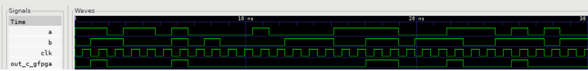
Fig. 9 Simulation Waveforms with Skywater PDK Circuit Model
We have now verified that the Skywater PDK Cell Library has been instantiated and bound to the OpenFPGA architecture file. If you have any problems, please Contact us.