Creating Spypads Using XML Syntax
Introduction
- In this tutorial, we will
Show the XML syntax for global outputs
Showcase an example with spypads
Modify an existing architecture to incorporate spypads
Verify correctness through GTKWave
Through this tutorial, we will show how to create spypads in OpenFPGA.
Spypads are physical output pins on a FPGA chip through which you can read out internal signals when doing silicon-level debugging. The XML syntax for spypads and other global signals can be found on our Circuit Library documentation page.
To create a spypad, the port type needs to be set to output and is_global and is_io need to be set to true:
<port type="output" is_global="true" is_io="true"/>
When the port is syntactically correct, the outputs are independently wired from different instances to separated FPGA outputs and would physically look like General-purpose outputs as separated FPGA I/Os
Pre-Built Spypads
An OpenFPGA architecture file that contains spypads and has a task that references it is the k6_frac_N10_adder_register_scan_chain_depop50_spypad_40nm_openfpga.xml
file. We can view k6_frac_N10_adder_register_scan_chain_depop50_spypad_40nm_openfpga.xml by entering the following command at the root directory of OpenFPGA:
emacs openfpga_flow/openfpga_arch/k6_frac_N10_adder_register_scan_chain_depop50_spypad_40nm_openfpga.xml
In this architecture file, the output ports of a 6-input Look-Up Table (LUT) are defined as spypads using the XML syntax is_global and is_io. As a result, all of the outputs from the 6-input LUT will be visible in the top-level module. The output ports to the 6-input LUT are declared from LINE181 to LINE183 and belong to the frac_lut6_spypad circuit_model that begins at LINE172.
<circuit_model type="lut" name="frac_lut6_spypad" prefix="frac_lut6_spypad" dump_structural_verilog="true">
   <design_technology type="cmos" fracturable_lut="true"/>
   <input_buffer exist="true" circuit_model_name="INVTX1"/>
   <output_buffer exist="true" circuit_model_name="INVTX1"/>
   <lut_input_inverter exist="true" circuit_model_name="INVTX1"/>
   <lut_input_buffer exist="true" circuit_model_name="buf4"/>
   <lut_intermediate_buffer exist="true" circuit_model_name="buf4" location_map="-1-1-"/>
   <pass_gate_logic circuit_model_name="TGATE"/>
   <port type="input" prefix="in" size="6" tri_state_map="----11" circuit_model_name="OR2"/>
   LINE181 <port type="output" prefix="lut4_out" size="4" lut_frac_level="4" lut_output_mask="0,1,2,3" is_global="true" is_io="true"/>
   LINE182 <port type="output" prefix="lut5_out" size="2" lut_frac_level="5" lut_output_mask="0,1" is_global="true" is_io="true"/>
   LINE183 <port type="output" prefix="lut6_out" size="1" lut_output_mask="0" is_global="true" is_io="true"/>
   <port type="sram" prefix="sram" size="64"/>
   <port type="sram" prefix="mode" size="2" mode_select="true" circuit_model_name="DFFR" default_val="1"/>
</circuit_model>
The spypads are instantiated in the top-level verilog module fpga_top.v. fpga_top.v is automatically generated when we run our task from the OpenFPGA root
directory. However, we need to modify the task configuration file to run the full testbench instead of the formal testbench to view the spypads’ waveforms in
GTKWave.
Note
To read about the differences between the formal testbench and the full testbench, please visit our page on testbenches: Testbench.
To open the task configuration file, run this command from the root directory of OpenFPGA:
emacs openfpga_flow/tasks/fpga_verilog/spypad/config/task.conf
The last line of the task configuration file (LINE44) sets the formal testbench to be the desired testbench. To use the full testbench, comment out LINE44. The file will look like this when finished:
 1# = = = = = = = = = = = = = = = = = = = = = = = = = = = = = = = = = = = = = = =
 2# Configuration file for running experiments
 3# = = = = = = = = = = = = = = = = = = = = = = = = = = = = = = = = = = = = = = =
 4# timeout_each_job : FPGA Task script splits fpga flow into multiple jobs
 5# Each job execute fpga_flow script on combination of architecture & benchmark
 6# timeout_each_job is timeout for each job
 7# = = = = = = = = = = = = = = = = = = = = = = = = = = = = = = = = = = = = = = =
 8
 9[GENERAL]
10run_engine=openfpga_shell
11power_tech_file = ${PATH:OPENFPGA_PATH}/openfpga_flow/tech/PTM_45nm/45nm.xml
12power_analysis = true
13spice_output=false
14verilog_output=true
15timeout_each_job = 20*60
16fpga_flow=vpr_blif
17
18[OpenFPGA_SHELL]
19openfpga_shell_template=${PATH:OPENFPGA_PATH}/openfpga_flow/openfpga_shell_scripts/example_script.openfpga
20openfpga_arch_file=${PATH:OPENFPGA_PATH}/openfpga_flow/openfpga_arch/k6_frac_N10_adder_register_scan_chain_depop50_spypad_40nm_openfpga.xml
21openfpga_sim_setting_file=${PATH:OPENFPGA_PATH}/openfpga_flow/openfpga_simulation_settings/auto_sim_openfpga.xml
22
23[ARCHITECTURES]
24arch0=${PATH:OPENFPGA_PATH}/openfpga_flow/vpr_arch/k6_frac_N10_tileable_adder_register_scan_chain_depop50_spypad_40nm.xml
25
26[BENCHMARKS]
27bench0=${PATH:OPENFPGA_PATH}/openfpga_flow/benchmarks/micro_benchmark/and2/and2.blif
28# Cannot pass automatically. Need change in .v file to match ports
29# When passed, we can replace the and2 benchmark
30#bench0=${PATH:OPENFPGA_PATH}/openfpga_flow/benchmarks/micro_benchmark/test_mode_low/test_mode_low.blif
31
32[SYNTHESIS_PARAM]
33bench0_top = and2
34bench0_act = ${PATH:OPENFPGA_PATH}/openfpga_flow/benchmarks/micro_benchmark/and2/and2.act
35bench0_verilog = ${PATH:OPENFPGA_PATH}/openfpga_flow/benchmarks/micro_benchmark/and2/and2.v
36
37#bench0_top = test_mode_low
38#bench0_act = ${PATH:OPENFPGA_PATH}/openfpga_flow/benchmarks/micro_benchmark/test_mode_low/test_mode_low.act
39#bench0_verilog = ${PATH:OPENFPGA_PATH}/openfpga_flow/benchmarks/micro_benchmark/test_mode_low/test_mode_low.v
40bench0_chan_width = 300
41
42[SCRIPT_PARAM_MIN_ROUTE_CHAN_WIDTH]
43end_flow_with_test=
44#vpr_fpga_verilog_formal_verification_top_netlist=
Our OpenFPGA task will now run the full testbench. We run the task with the following command from the root directory of OpenFPGA:
python3 openfpga_flow/scripts/run_fpga_task.py fpga_verilog/spypad --debug --show_thread_logs
Note
Python 3.8 or later is required to run this task
We can now see the instantiation of these spypads in fpga_top.v and luts.v. We will start by viewing luts.v with the following command:
emacs openfpga_flow/tasks/fpga_verilog/spypad/latest/k6_frac_N10_tileable_adder_register_scan_chain_depop50_spypad_40nm/and2/MIN_ROUTE_CHAN_WIDTH/SRC/sub_module/luts.verilog
The spypads are coming from the frac_lut6_spypad circuit model. In luts.v, the frac_lut6_spypad module is defined around LINE150 and looks as follows:
module frac_lut6_spypad(in,
sram,
sram_inv,
mode,
mode_inv,
lut4_out,
lut5_out,
lut6_out);
//----- INPUT PORTS -----
input [0:5] in;
//----- INPUT PORTS -----
input [0:63] sram;
//----- INPUT PORTS -----
input [0:63] sram_inv;
//----- INPUT PORTS -----
input [0:1] mode;
//----- INPUT PORTS -----
input [0:1] mode_inv;
//----- OUTPUT PORTS -----
output [0:3] lut4_out;
//----- OUTPUT PORTS -----
output [0:1] lut5_out;
//----- OUTPUT PORTS -----
output [0:0] lut6_out;
The fpga_top.v file has some similarities. We can view the fpga_top.v file by running the following command:
emacs openfpga_flow/tasks/fpga_verilog/spypad/latest/k6_frac_N10_tileable_adder_register_scan_chain_depop50_spypad_40nm/and2/MIN_ROUTE_CHAN_WIDTH/SRC/fpga_top.v
If we look at the module definition and ports of fpga_top.v we should see the following:
module fpga_top(pReset,
             prog_clk,
             TESTEN,
             set,
             reset,
             clk,
             gfpga_pad_frac_lut6_spypad_lut4_out,
             gfpga_pad_frac_lut6_spypad_lut5_out,
             gfpga_pad_frac_lut6_spypad_lut6_out,
             gfpga_pad_GPIO_PAD,
             ccff_head,
             ccff_tail);
//----- GLOBAL PORTS -----
input [0:0] pReset;
//----- GLOBAL PORTS -----
input [0:0] prog_clk;
//----- GLOBAL PORTS -----
input [0:0] TESTEN;
//----- GLOBAL PORTS -----
input [0:0] set;
//----- GLOBAL PORTS -----
input [0:0] reset;
//----- GLOBAL PORTS -----
input [0:0] clk;
//----- GPOUT PORTS -----
output [0:3] gfpga_pad_frac_lut6_spypad_lut4_out;
//----- GPOUT PORTS -----
output [0:1] gfpga_pad_frac_lut6_spypad_lut5_out;
//----- GPOUT PORTS -----
output [0:0] gfpga_pad_frac_lut6_spypad_lut6_out;
//----- GPIO PORTS -----
inout [0:7] gfpga_pad_GPIO_PAD;
//----- INPUT PORTS -----
input [0:0] ccff_head;
//----- OUTPUT PORTS -----
output [0:0] ccff_tail;
Using General-purpose outputs as separated FPGA I/Os as a guide, we can relate our task like Fig. 10

Fig. 10 An illustrative example of the lut6 spypad sourced from inside a logic element.
We can view testbench waveforms with GTKWave by running the following command from the root directory:
gtkwave openfpga_flow/tasks/fpga_verilog/spypad/latest/k6_frac_N10_tileable_adder_register_scan_chain_depop50_spypad_40nm/and2/MIN_ROUTE_CHAN_WIDTH/and2_formal.vcd &
Note
Information on GTKWave can be found on our documentation page located here: From Verilog to Verification
The waveforms will appear similar to Fig. 11
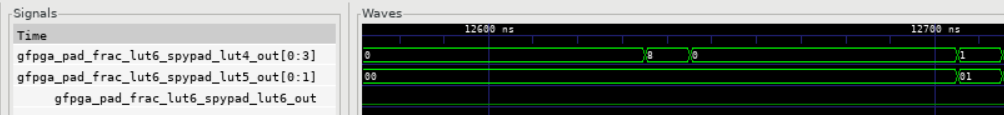
Fig. 11 Waveforms of frac_lut6 spypads
Building Spypads
We will modify the k6_frac_N10_adder_chain_40nm_openfpga.xml file found in OpenFPGA to expose the sumout output from the ADDF module. We can start modifying the file by running the following command:
emacs openfpga_flow/openfpga_arch/k6_frac_N10_adder_chain_40nm_openfpga.xml
Replace LINE214 with the following:
<port type="output" prefix="sumout" lib_name="SUM" size="1" is_global=”true” is_io=”true”/>
sumout is now a global output. sumout will show up in the fpga_top.v file and will have waveforms in GTKWave if we run the full testbench. To run the
full testbench, we have to modify the hard_adder configuration file:
emacs openfpga_flow/tasks/fpga_verilog/adder/hard_adder/config/task.conf
Comment out the last line of the file to run the full testbench:
#vpr_fpga_verilog_formal_verification_top_netlist=
We now run the task to see our changes:
python3 openfpga_flow/scripts/run_fpga_task.py fpga_verilog/adder/hard_adder --debug --show_thread_logs
We can view the global ports in fpga_top.v by running the following command:
emacs openfpga_flow/tasks/fpga_verilog/adder/hard_adder/run064/k6_frac_N10_tileable_adder_chain_40nm/and2/MIN_ROUTE_CHAN_WIDTH/SRC/fpga_top.v
The fpga_top.v should have the following in its module definition:
module fpga_top(pReset,
             prog_clk,
             set,
             reset,
             clk,
             gfpga_pad_ADDF_sumout,
             gfpga_pad_GPIO_PAD,
             ccff_head,
             ccff_tail);
//----- GLOBAL PORTS -----
input [0:0] pReset;
//----- GLOBAL PORTS -----
input [0:0] prog_clk;
//----- GLOBAL PORTS -----
input [0:0] set;
//----- GLOBAL PORTS -----
input [0:0] reset;
//----- GLOBAL PORTS -----
input [0:0] clk;
//----- GPOUT PORTS -----
output [0:19] gfpga_pad_ADDF_sumout;
The architecture will now look like Fig. 12

Fig. 12 An illustrative example of the sumout spypad sourced from an adder inside a logic element. There are 10 logic elements in a CLB, and we are looking at the 1st logic element.
We can view the waveform by running GTKWave:
gtkwave openfpga_flow/tasks/fpga_verilog/adder/hard_adder/latest/k6_frac_N10_tileable_adder_chain_40nm/and2/MIN_ROUTE_CHAN_WIDTH/and2_formal.vcd &
The waveform should have some changes to its value. An example of what it may look like is displayed in Fig. 13
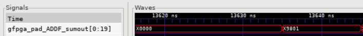
Fig. 13 Waveforms of sumout spypad
Conclusion
In this tutorial, we have shown how to build spypads into OpenFPGA Architectures using XML Syntax. If you have any issues, feel free to Contact us.