Additional Syntax to Original VPR XML
Warning
Note this is only applicable to VPR8!
Models, Complex blocks and Physical Tiles
Each <pb_type> should contain a <mode> that describes the physical implementation of the <pb_type>. Note that this is fully compatible to the VPR architecture XML syntax.
Note
<model> should include the models that describe the primitive <pb_type> in physical mode.
Note
Currently, OpenFPGA only supports 1 <equivalent_sites> to be defined under each <tile>
- <mode disable_packing="<bool">/>
OpenFPGA allows users to define it a mode is disabled for VPR packer. By default, the
disable_packingis set tofalse. This is mainly used for the mode that describes the physical implementation, which is typically not packable. Disable it in the packing and signficantly accelerate the packing runtime.Note
Once a mode is disabled in packing, its child modes will be disabled as well.
Note
The following syntax is only available in OpenFPGA!
We allow more flexible pin location assignment when a <tile> has a capacity > 1.
User can specify the location using the index of instance, e.g.,
<tile name="io_bottom" capacity="6" area="0">
  <equivalent_sites>
    <site pb_type="io"/>
  </equivalent_sites>
  <input name="outpad" num_pins="1"/>
  <output name="inpad" num_pins="1"/>
  <fc in_type="frac" in_val="0.15" out_type="frac" out_val="0.10"/>
  <pinlocations pattern="custom">
    <loc side="top">io_bottom[0:1].outpad io_bottom[0:3].inpad io_bottom[2:5].outpad io_bottom[4:5].inpad</loc>
  </pinlocations>
</tile>
Layout
<layout> may include additioinal syntax to enable tileable routing resource graph generation
- tileable="<bool>"
Turn
on/offtileable routing resource graph generator.Tileable routing architecture can minimize the number of unique modules in FPGA fabric to be physically implemented.
Technical details can be found in [TGAG19].
Note
Strongly recommend to enable the tileable routing architecture when you want to PnR large FPGA fabrics, which can effectively reduce the runtime.
- through_channel="<bool>"
Allow routing channels to pass through multi-width and multi-height programable blocks. This is mainly used in heterogeneous FPGAs to increase routability, as illustrated in Fig. 14. By default, it is
false.
Fig. 14 Impact on routing architecture when through channel in multi-width and multi-height programmable blocks: (a) disabled; (b) enabled.
Warning
Do NOT enable
through_channelif you are not using the tileable routing resource graph generator!Warning
You cannot use
spreadpin location for theheight > 1orwidth >1tiles when using the tileable routing resource graph!!! Otherwise, it will cause undriven pins in your device!!!
- shrink_boundary="<bool>"
Remove all the routing wires in empty regions. This is mainly used in non-rectangle FPGAs to avoid redundant routing wires in blank area, as illustrated in Fig. 15. By default, it is
false.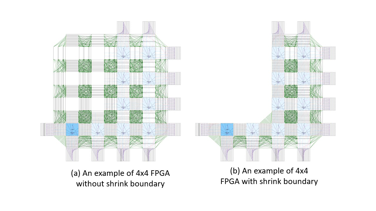
Fig. 15 Impact on routing architecture when shrink-boundary: (a) disabled; (b) enabled.
Warning
Do NOT enable
shrink_boundaryif you are not using the tileable routing resource graph generator!
- perimeter_cb="<bool>"
Allow connection blocks to appear around the perimeter programmable block (mainly I/Os). This is designed to enhance routability of I/Os on perimeter. Also strongly recommended when programmable clock network is required to touch clock pins on I/Os. As illustrated in Fig. 16, routing tracks can access three sides of each I/O when perimeter connection blocks are created. By default, it is
false.
Warning
When enabled, please only place outputs at one side of I/Os. For example, outputs of an I/O on the top side can only occur on the bottom side of the I/O tile. Otherwise, routability loss may be expected, leading to some pins cannot be reachable. Enable the opin2all_sides to recover routability loss.

Fig. 16 Impact on routing architecture when perimeter connection blocks are : (a) disabled; (b) enabled.
Warning
Do NOT enable perimeter_cb if you are not using the tileable routing resource graph generator!
- opin2all_sides="<bool>"
Allow each output pin of a programmable block to drive the routing tracks on all the sides of its adjacent switch block (see an illustrative example in Fig. 17). This can improve the routability of an FPGA fabric with an increase in the sizes of routing multiplexers in each switch block. By default, it is
false.
Fig. 17 Impact on routing architecture when the opin-to-all-sides: (a) disabled; (b) enabled.
Warning
Do NOT enable
opin2all_sidesif you are not using the tileable routing resource graph generator!
- concat_wire="<bool>"
In each switch block, allow each routing track which ends to drive another routing track on the opposite side, as such a wire can be continued in the same direction (see an illustrative example in
fig_concat_wire). In other words, routing wires can be concatenated in the same direction across an FPGA fabric. This can improve the routability of an FPGA fabric with an increase in the sizes of routing multiplexers in each switch block. By default, it isfalse.
Fig. 18 Impact on routing architecture when the wire concatenation: (a) disabled; (b) enabled.
Warning
Do NOT enable
concat_wireif you are not using the tileable routing resource graph generator!
- concat_pass_wire="<bool>"
In each switch block, allow each routing track which passes to drive another routing track on the opposite side, as such a pass wire can be continued in the same direction (see an illustrative example in
fig_concat_pass_wire). This can improve the routability of an FPGA fabric with an increase in the sizes of routing multiplexers in each switch block. By default, it isfalse.Warning
Please enable this option if you are looking for device support which is created by any release which is before v1.1.541!!!

Fig. 19 Impact on routing architecture when the pass wire concatenation: (a) disabled; (b) enabled.
Warning
Do NOT enable
concat_pass_wireif you are not using the tileable routing resource graph generator!
A quick example to show tileable routing is enabled, other options, e.g., through channels are disabled:
<layout tileable="true" through_channel="false" shrink_boundary="false" opin2all_sides="false" concat_wire="false" concat_pass_wire="false">
</layout>
Switch Block
<switch_block> may include addition syntax to enable different connectivity for pass tracks
- sub_type="<string>"
Connecting type for pass tracks in each switch block The supported connecting patterns are
subset,universalandwilton, being the same as VPR capability If not specified, the pass tracks will the same connecting patterns as start/end tracks, which are defined intype
- sub_Fs="<int>"
Connectivity parameter for pass tracks in each switch block. Must be a multiple of 3. If not specified, the pass tracks will the same connectivity as start/end tracks, which are defined in
fs
- A quick example which defines a switch block
Starting/ending routing tracks are connected in the
wiltonpatternEach starting/ending routing track can drive 3 other starting/ending routing tracks
Passing routing tracks are connected in the
subsetpatternEach passing routing track can drive 6 other starting/ending routing tracks
<device>
  <switch_block type="wilton" fs="3" sub_type="subset" sub_fs="6"/>
</device>
Routing Segments
OpenFPGA suggests users to give explicit names for each routing segement in <segmentlist>
This is used to link circuit_model to routing segments.
A quick example which defines a length-4 uni-directional routing segment called L4 :
<segmentlist>
  <segment name="L4" freq="1" length="4" type="undir"/>
</segmentlist>
Note
Currently, OpenFPGA only supports uni-directional routing architectures