Circuit model examples
As circuit model in different types have various special syntax.
Here, we will provide detailed examples on each type of circuit_model.
These examples may be considered as template for users to craft their own circuit_model.
Inverters and Buffers
Template
<circuit_model type="inv_buf" name="<string>" prefix="<string>" netlist="<string>" is_default="<int>">
  <design_technology type="cmos" topology="<string>" size="<int>" num_level="<int>" f_per_stage="<float>"/>
  <port type="input" prefix="<string>" size="<int>"/>
  <port type="output" prefix="<string>" size="<int>"/>
</circuit_model>
- <design_technology type="cmos" topology="<string>" size="<int>" num_level="<int>" f_per_stage="<float>"/>
topology="inverter|buffer"Specify the type of this component, can be either an inverter or a buffer.size="<int>"Specify the driving strength of inverter/buffer. For a buffer, the size is the driving strength of the inverter at the second level. Note that we consider a two-level structure for a buffer here.num_level="<int>"Define the number of levels of a tapered inverter/buffer. This is required when users need an inverter or a buffer consisting of >2 stagesf_per_stage="<float>"Define the ratio of driving strength between the levels of a tapered inverter/buffer. Default value is 4.
Inverter 1x Example
Fig. 42 is the inverter symbol depicted in this example.
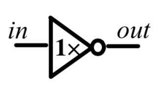
Fig. 42 Classical inverter 1x symbol.
The XML code describing this inverter is:
<circuit_model type="inv_buf" name="inv1x" prefix="inv1x">
  <design_technology type="cmos" topology="inverter" size="1"/>
  <port type="input" prefix="in" size="1"/>
  <port type="output" prefix="out" size="1"/>
</circuit_model>
This example shows:
The topology chosen as inverter
Size of 1 for the output strength
The tapered parameter is not declared and is
falseby default
Power-gated Inverter 1x example
The XML code describing an inverter which can be power-gated by the control signals EN and ENB :
<circuit_model type="inv_buf" name="INVTX1" prefix="INVTX1">
  <design_technology type="cmos" topology="inverter" size="3" power_gated="true"/>
  <port type="input" prefix="in" size="1" lib_name="I"/>
  <port type="input" prefix="EN" size="1" lib_name="EN" is_global="true" default_val="0" is_config_enable="true"/>
  <port type="input" prefix="ENB" size="1" lib_name="ENB" is_global="true" default_val="1" is_config_enable="true"/>
  <port type="output" prefix="out" size="1" lib_name="Z"/>
</circuit_model>
Note
For power-gated inverters: all the control signals must be set as config_enable so that the testbench generation will generate testing waveforms. If the power-gated inverters are auto-generated, all the config_enable signals must be global signals as well. If the power-gated inverters come from user-defined netlists, restrictions on global signals are free.
Buffer 2x example
Fig. 43 is the buffer symbol depicted in this example.
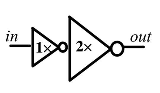
Fig. 43 Buffer made by two inverter, with an output strength of 2.
The XML code describing this buffer is:
<circuit_model type="inv_buf" name="buf2" prefix="buf2">
  <design_technology type="cmos" topology="buffer" size="2"/>
  <port type="input" prefix="in" size="1"/>
  <port type="output" prefix="out" size="1"/>
</circuit_model>
- This example shows:
The topology chosen as buffer
Size of 2 for the output strength
The tapered parameter is not declared and is
falseby default
Power-gated Buffer 4x example
The XML code describing a buffer which can be power-gated by the control signals EN and ENB :
<circuit_model type="inv_buf" name="buf_4x" prefix="buf_4x">
  <design_technology type="cmos" topology="buffer" size="4" power_gated="true"/>
  <port type="input" prefix="in" size="1" lib_name="I"/>
  <port type="input" prefix="EN" size="1" lib_name="EN" is_global="true" default_val="0" is_config_enable="true"/>
  <port type="input" prefix="ENB" size="1" lib_name="ENB" is_global="true" default_val="1" is_config_enable="true"/>
  <port type="output" prefix="out" size="1" lib_name="Z"/>
</circuit_model>
Note
For power-gated buffers: all the control signals must be set as config_enable so that the testbench generation will generate testing waveforms. If the power-gated buffers are auto-generated, all the config_enable signals must be global signals as well. If the power-gated buffers come from user-defined netlists, restrictions on global signals are free.
Tapered inverter 16x example
Fig. 44 is the tapered inverter symbol depicted this example.
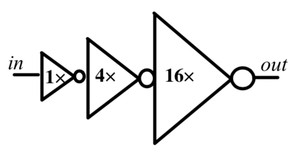
Fig. 44 Inverter with high output strength made by 3 stage of inverter.
The XML code describing this inverter is:
<circuit_model type="inv_buf" name="tapdrive4" prefix="tapdrive4">
  <design_technology type="cmos" topology="inverter" size="1" num_level="3" f_per_stage="4"/>
  <port type="input" prefix="in" size="1"/>
  <port type="output" prefix="out" size="1"/>
</circuit_model>
- This example shows:
The topology chosen as inverter
Size of 1 for the first stage output strength
The number of stage is set to 3 by
f_per_stage is set to 4. As a result, 2nd stage output strength is 4x, and the 3rd stage output strength is 16x.
Tapered buffer 64x example
The XML code describing a 4-stage buffer is:
<circuit_model type="inv_buf" name="tapbuf_16x" prefix="tapbuf_16x">
  <design_technology type="cmos" topology="buffer" size="1" num_level="4" f_per_stage="4"/>
  <port type="input" prefix="in" size="1"/>
  <port type="output" prefix="out" size="1"/>
</circuit_model>
- This example shows:
The topology chosen as buffer
Size of 1 for the first stage output strength
The number of stage is set to 4 by
f_per_stage is set to 2. As a result, 2nd stage output strength is 4*, the 3rd stage output strength is 16*, and the 4th stage output strength is 64x.
Pass-gate Logic
Template
<circuit_model type="pass_gate" name="<string>" prefix="<string>" netlist="<string>" is_default="<int>">
  <design_technology type="cmos" topology="<string>" nmos_size="<float>" pmos_size="<float>"/>
  <input_buffer exist="false"/>
  <output_buffer exist="false"/>
  <port type="input" prefix="<string>" size="<int>"/>
  <port type="output" prefix="<string>" size="<int>"/>
</circuit_model>
Note
The port sequence really matters! And all the input ports must have an input size of 1!
The first input must be the datapath input, e.g.,
in.The second input must be the select input, e.g.,
sel.The third input (if applicable) must be the inverted select input, e.g.,
selb.
Warning
Please do NOT add input and output buffers to pass-gate logic.
- <design_technology type="cmos" topology="<string>" nmos_size="<float>" pmos_size="<float>"/>
topology="transmission_gate|pass_transistor"Specify the circuit topology for the pass-gate logic. A transmission gate consists of a n-type transistor and a p-type transistor. The pass transistor consists of only a n-type transistor.nmos_size="<float>"the size of n-type transistor in a transmission gate or pass_transistor, expressed in terms of the minimum widthmin_widthdefined in the transistor model in Technology library.pmos_size="<float>"the size of p-type transistor in a transmission gate, expressed in terms of the minimum widthmin_widthdefined in the transistor model in Technology library.
Note
nmos_size and pmos_size are required for FPGA-SPICE
Transmission-gate Example
Fig. 45 is the pass-gate symbol depicted in this example.
Fig. 45 Pass-gate made by a p-type and a n-type transistors.
The XML code describing this pass-gate is:
<circuit_model type="pass_gate" name="tgate" prefix="tgate">
  <design_technology type="cmos" topology="transmission_gate" nmos_size="1" pmos_size="2"/>
  <port type="input" prefix="in" size="1"/>
  <port type="input" prefix="sram" size="1"/>
  <port type="input" prefix="sramb" size="1"/>
  <port type="output" prefix="out" size="1"/>
</circuit_model>
- This example shows:
A
transmission_gatebuilt with a n-type transistor in the size of 1 and a p-type transistor in the size of 2.3 inputs considered, 1 for datapath signal and 2 to turn on/off the transistors gates
Pass-transistor Example
Fig. 46 is the pass-gate symbol depicted in this example.
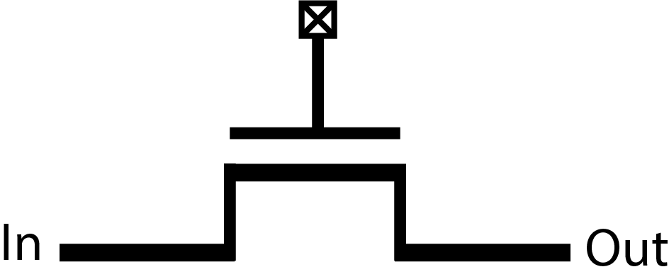
Fig. 46 Pass-gate made by a nmos transistor.
The XML code describing this pass-gate is:
<circuit_model type="pass_gate" name="t_pass" prefix="t_pass">
  <design_technology type="cmos" topology="pass_transistor"/>
  <port type="input" prefix="in" size="1"/>
  <port type="input" prefix="sram" size="1"/>
  <port type="output" prefix="out" size="1"/>
</circuit_model>
- This example shows:
A
pass_transistorbuild with a n-type transistor in the size of 12 inputs considered, 1 for datapath signal and 1 to turn on/off the transistor gate
SRAMs
Note
OpenFPGA does not auto-generate any netlist for SRAM cells. Users should define the HDL modeling in external netlists and ensure consistency to physical designs.
Template
<circuit_model type="sram" name="<string>" prefix="<string>" verilog_netlist="<string>" spice_netlist="<string>"/>
  <design_technology type="cmos"/>
  <input_buffer exist="<string>" circuit_model_name="<string>"/>
  <output_buffer exist="<string>" circuit_model_name="<string>"/>
  <port type="input" prefix="<string>" size="<int>"/>
  <port type="output" prefix="<string>" size="<int>"/>
</circuit_model>
Note
The circuit designs of SRAMs are highly dependent on the technology node and well optimized by engineers. Therefore, FPGA-Verilog/SPICE requires users to provide their customized SRAM Verilog/SPICE/Verilog netlists. A sample Verilog/SPICE netlist of SRAM can be found in the directory SpiceNetlists in the released package. FPGA-Verilog/SPICE assumes that all the LUTs and MUXes employ the SRAM circuit design. Therefore, currently only one SRAM type is allowed to be defined.
Note
The information of input and output buffer should be clearly specified according to the customized Verilog/SPICE netlist! The existence of input/output buffers will influence the decision in creating testbenches, which may leads to larger errors in power analysis.
SRAM with BL/WL
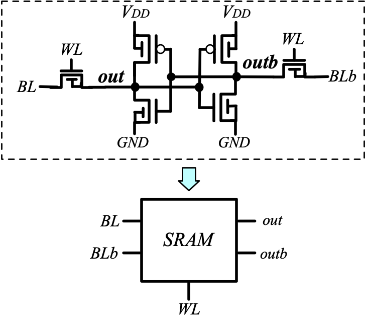
Fig. 47 An example of a SRAM with Bit-Line (BL) and Word-Line (WL) control signals
The following XML codes describes the SRAM cell shown in Fig. 47.
<circuit_model type="sram" name="sram_blwl" prefix="sram_blwl" verilog_netlist="sram.v" spice_netlist="sram.sp"/>
  <design_technology type="cmos"/>
  <input_buffer exist="false"/>
  <output_buffer exist="false"/>
  <port type="bl" prefix="bl" size="1"/>
  <port type="blb" prefix="blb" size="1"/>
  <port type="wl" prefix="wl" size="1"/>
  <port type="output" prefix="out" size="1"/>
  <port type="output" prefix="outb" size="1"/>
</circuit_model>
Note
OpenFPGA always assume that a WL port should be the write/read enable signal, while a BL port is the data input.
Note
When the memory_bank type of configuration procotol is specified, SRAM modules should have a BL and a WL.
SRAM with BL/WL/WLR

Fig. 48 An example of a SRAM with Bit-Line (BL), Word-Line (WL) and WL read control signals
The following XML codes describes the SRAM cell shown in Fig. 48.
<circuit_model type="sram" name="sram_blwlr" prefix="sram_blwlr" verilog_netlist="sram.v" spice_netlist="sram.sp"/>
  <design_technology type="cmos"/>
  <input_buffer exist="false"/>
  <output_buffer exist="false"/>
  <port type="bl" prefix="bl" size="1"/>
  <port type="wl" prefix="wl" size="1"/>
  <port type="wlr" prefix="wlr" size="1"/>
  <port type="output" prefix="out" size="1"/>
  <port type="output" prefix="outb" size="1"/>
</circuit_model>
Note
OpenFPGA always assume that a WL port should be the write enable signal, a WLR port should be the read enable signal, while a BL port is the data input.
Note
When the memory_bank type of configuration procotol is specified, SRAM modules should have a BL and a WL. WLR is optional
Configurable Latch

Fig. 49 An example of a SRAM-based configurable latch with Bit-Line (BL) and Word-Line (WL) control signals
The following XML codes describes the configurable latch shown in Fig. 49.
<circuit_model type="sram" name="config_latch" prefix="config_latch" verilog_netlist="sram.v" spice_netlist="sram.sp"/>
  <design_technology type="cmos"/>
  <input_buffer exist="false"/>
  <output_buffer exist="false"/>
  <port type="clock" prefix="clk" size="1"/>
  <port type="bl" prefix="bl" size="1"/>
  <port type="wl" prefix="wl" size="1"/>
  <port type="output" prefix="out" size="1"/>
  <port type="output" prefix="outb" size="1"/>
</circuit_model>
Note
OpenFPGA always assume that a WL port should be the write/read enable signal, while a BL port is the data input.
Note
When the frame_based type of configuration procotol is specified, the configurable latch or a SRAM with BL and WL should be specified.
Logic gates
The circuit model in the type of gate aims to support direct mapping to standard cells or customized cells provided by technology vendors or users.
Template
<circuit_model type="gate" name="<string>" prefix="<string>" spice_netlist="<string>" verilog_netlist="<string>"/>
  <design_technology type="cmos" topology="<string>"/>
  <input_buffer exist="<string>" circuit_model_name="<string>"/>
  <output_buffer exist="<string>" circuit_model_name="<string>"/>
  <port type="input" prefix="<string>" lib_name="<string>" size="<int>"/>
  <port type="output" prefix="<string>" lib_name="<string>" size="<int>"/>
</circuit_model>
- <design_technology type="cmos" topology="<string>"/>
topology="AND|OR|MUX2"Specify the logic functionality of a gate. As for standard cells, the size of each port is limited to 1. Currently, only 2-input and single-output logic gates are supported.
Note
The port sequence really matters for MUX2 logic gates!
The first two inputs must be the datapath inputs, e.g.,
in0andin1.The third input must be the select input, e.g.,
sel.
2-input AND Gate
<circuit_model type="gate" name="AND2" prefix="AND2" is_default="true">
  <design_technology type="cmos" topology="AND"/>
  <input_buffer exist="false"/>
  <output_buffer exist="false"/>
  <port type="input" prefix="a" size="1"/>
  <port type="input" prefix="b" size="1"/>
  <port type="output" prefix="out" size="1"/>
  <delay_matrix type="rise" in_port="a b" out_port="out">
    10e-12 8e-12
  </delay_matrix>
  <delay_matrix type="fall" in_port="a b" out_port="out">
    10e-12 7e-12
  </delay_matrix>
</circuit_model>
- This example shows:
A 2-input AND gate without any input and output buffers
Propagation delay from input
atooutis 10ps in rising edge and and 8ps in falling edgePropagation delay from input
btooutis 10ps in rising edge and 7ps in falling edge
2-input OR Gate
<circuit_model type="gate" name="OR2" prefix="OR2" is_default="true">
  <design_technology type="cmos" topology="OR"/>
  <input_buffer exist="false"/>
  <output_buffer exist="false"/>
  <port type="input" prefix="a" size="1"/>
  <port type="input" prefix="b" size="1"/>
  <port type="output" prefix="out" size="1"/>
  <delay_matrix type="rise" in_port="a b" out_port="out">
    10e-12 8e-12
  </delay_matrix>
  <delay_matrix type="fall" in_port="a b" out_port="out">
    10e-12 7e-12
  </delay_matrix>
</circuit_model>
- This example shows:
A 2-input OR gate without any input and output buffers
Propagation delay from input
atooutis 10ps in rising edge and and 8ps in falling edgePropagation delay from input
btooutis 10ps in rising edge and 7ps in falling edge
MUX2 Gate
<circuit_model type="gate" name="MUX2" prefix="MUX2" is_default="true" verilog_netlist="sc_mux.v">
  <design_technology type="cmos" topology="MUX2"/>
  <input_buffer exist="false"/>
  <output_buffer exist="false"/>
  <port type="input" prefix="in0" lib_name="B" size="1"/>
  <port type="input" prefix="in1" lib_name="A" size="1"/>
  <port type="input" prefix="sel" lib_name="S" size="1"/>
  <port type="output" prefix="out" lib_name="Y" size="1"/>
</circuit_model>
- This example shows:
A 2-input MUX gate with two inputs
in0andin1, a select portseland an output portoutThe Verilog of MUX2 gate is provided by the user in the netlist
sc_mux.vThe use of
lib_nameto bind to a Verilog module with different port names.When binding to the Verilog module, the inputs will be swapped. In other words,
in0of the circuit model will be wired to the inputBof the MUX2 cell, whilein1of the circuit model will be wired to the inputAof the MUX2 cell.
Note
OpenFPGA requires a fixed truth table for the MUX2 gate. When the select signal sel is enabled, the first input, i.e., in0, will be propagated to the output, i.e., out. If your standard cell provider does not offer the exact truth table, you can simply swap the inputs as shown in the example.
Multiplexers
Template
<circuit_model type="mux" name="<string>" prefix="<string>">
  <design_technology type="<string>" structure="<string>" num_level="<int>" add_const_input="<bool>" const_input_val="<int>" local_encoder="<bool>"/>
  <input_buffer exist="<string>" circuit_model_name="<string>"/>
  <output_buffer exist="<string>" circuit_model_name="<string>"/>
  <pass_gate_logic type="<string>" circuit_model_name="<string>"/>
  <port type="input" prefix="<string>" size="<int>"/>
  <port type="output" prefix="<string>" size="<int>"/>
  <port type="sram" prefix="<string>" size="<int>"/>
</circuit_model>
Note
user-defined Verilog/SPICE netlists are not currently supported for multiplexers.
- <design_technology type="<string>" structure="<string>" num_level="<int>" add_const_input="<bool>" const_input_val="<int>" local_encoder="<bool>"/>
structure="tree|multi_level|one_level"Specify the multiplexer structure for a multiplexer. The structure option is only valid for SRAM-based multiplexers. For RRAM-based multiplexers, currently we only support the one_level structurenum_level="<int>"Specify the number of levels whenmulti_levelstructure is selected.add_const_input="true|false"Specify if an extra input should be added to the multiplexer circuits. For example, an 4-input multiplexer will be turned to a 5-input multiplexer. The extra input will be wired to a constant value, which can be specified through the XML syntaxconst_input_val.Note
Adding an extra constant input will help reducing the leakage power of FPGA and parasitic signal activities, with a limited area overhead.
const_input_val="0|1"Specify the constant value, to which the extra input will be connected. By default it is 0. This syntax is only valid when theadd_const_inputis set to true.local_encoder="true|false". Specify if a local encoder should be added to the multiplexer circuits. The local encoder will interface the SRAM inputs of multiplexing structure and SRAMs. It can encode the one-hot codes (that drive the select port of multiplexing structure) to a binary code. For example, 8-bit00000001will be encoded to 3-bit000. This will help reduce the number of SRAM cells used in FPGAs as well as configuration time (especially for scan-chain configuration protocols). But it may cost an area overhead.Note
Local encoders are only applicable for one-level and multi-level multiplexers. Tree-like multiplexers are already encoded in their nature.
Note
A multiplexer should have only three types of ports, input, output and sram, which are all mandatory.
Note
For tree-like multiplexers, they can be built with standard cell MUX2. To enable this, users should define a circuit_model, which describes a 2-input multiplexer (See details and examples in how to define a logic gate using circuit_model. In this case, the circuit_model_name in the pass_gate_logic should be the name of MUX2 circuit_model.
Note
When multiplexers are not provided by users, the size of ports do not have to be consistent with actual numbers in the architecture.
One-level Multiplexer
Fig. 50 illustrates an example of multiplexer modelling, which consists of input/output buffers and a transmission-gate-based tree structure.
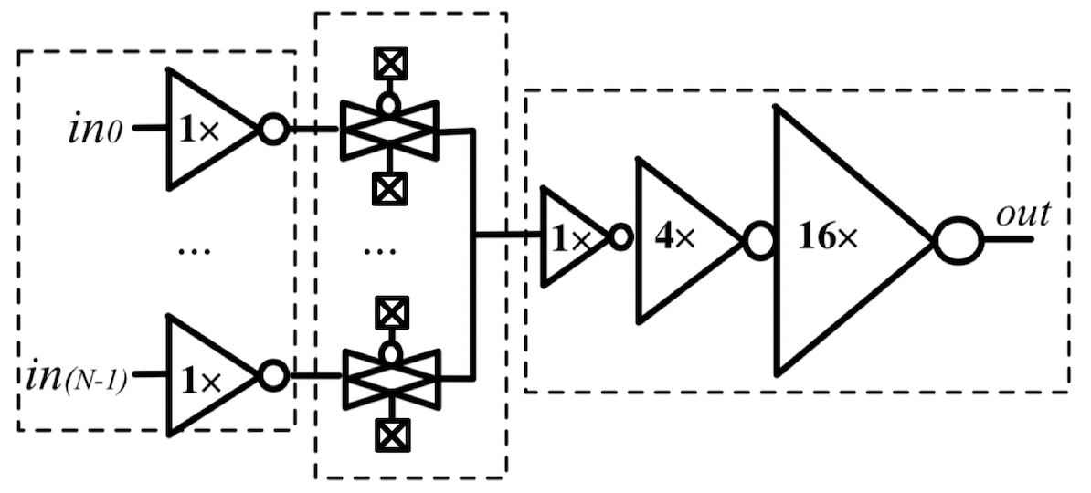
Fig. 50 An example of a one level multiplexer with transistor-level design parameters
The code describing this Multiplexer is:
<circuit_model type="mux" name="mux_1level" prefix="mux_1level">
  <design_technology type="cmos" structure="one_level"/>
  <input_buffer exist="on" circuit_model_name="inv1x"/>
  <output_buffer exist="on" circuit_model_name="tapbuf4"/>
  <pass_gate_logic circuit_model_name="tgate"/>
  <port type="input" prefix="in" size="4"/>
  <port type="output" prefix="out" size="1"/>
  <port type="sram" prefix="sram" size="4"/>
</circuit_model>
- This example shows:
A one-level 4-input CMOS multiplexer
All the inputs will be buffered using the circuit model
inv1xAll the outputs will be buffered using the circuit model
tapbuf4The multiplexer will be built by transmission gate using the circuit model
tgateThe multiplexer will have 4 inputs and 4 SRAMs to control which datapath to propagate
Tree-like Multiplexer
Fig. 51 illustrates an example of multiplexer modelling, which consists of input/output buffers and a transmission-gate-based tree structure.
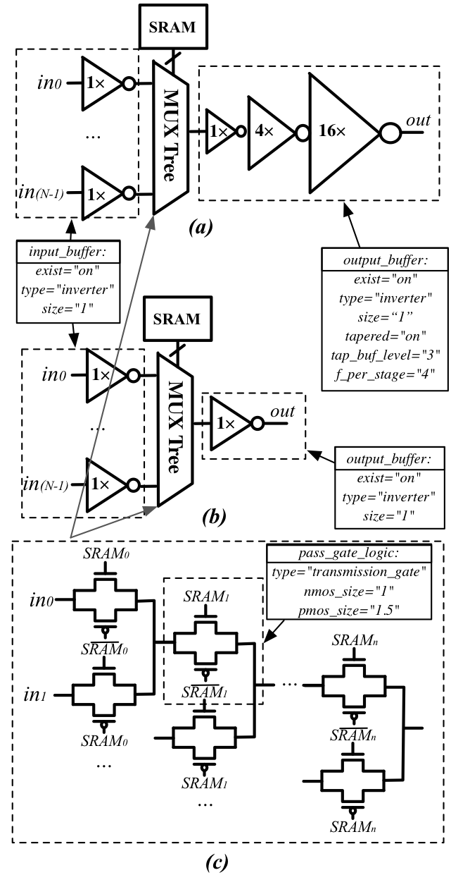
Fig. 51 An example of a tree-like multiplexer with transistor-level design parameters
If we arbitrarily fix the number of Mux entries at 4, the following code could illustrate (a):
<circuit_model type="mux" name="mux_tree" prefix="mux_tree">
  <design_technology type="cmos" structure="tree"/>
  <input_buffer exist="on" circuit_model_name="inv1x"/>
  <output_buffer exist="on" circuit_model_name="tapdrive4"/>
  <pass_gate_logic circuit_model_name="tgate"/>
  <port type="input" prefix="in" size="4"/>
  <port type="output" prefix="out" size="1"/>
  <port type="sram" prefix="sram" size="3"/>
</circuit_model>
- This example shows:
A tree-like 4-input CMOS multiplexer
All the inputs will be buffered using the circuit model
inv1xAll the outputs will be buffered using the circuit model
tapbuf4The multiplexer will be built by transmission gate using the circuit model
tgateThe multiplexer will have 4 inputs and 3 SRAMs to control which datapath to propagate
Standard Cell Multiplexer

Fig. 52 An example of a multiplexer built with standard cells: (a) all the MUX2 are the same; (b) the MUX2 at the last stage is a different one
<circuit_model type="mux" name="mux_stdcell" prefix="mux_stdcell">
  <design_technology type="cmos" structure="tree"/>
  <input_buffer exist="on" circuit_model_name="inv1x"/>
  <output_buffer exist="on" circuit_model_name="tapdrive4"/>
  <pass_gate_logic circuit_model_name="MUX2"/>
  <port type="input" prefix="in" size="4"/>
  <port type="output" prefix="out" size="1"/>
  <port type="sram" prefix="sram" size="3"/>
</circuit_model>
- This example shows (see an illustative example in Fig. 52 (a)):
A tree-like 4-input CMOS multiplexer built by the standard cell
MUX2All the inputs will be buffered using the circuit model
inv1xAll the outputs will be buffered using the circuit model
tapbuf4The multiplexer will have 4 inputs and 3 SRAMs to control which datapath to propagate
Alternatively, user can specify a different standard cell MUX2 at the last stage.
<circuit_model type="mux" name="mux_stdcell" prefix="mux_stdcell">
  <design_technology type="cmos" structure="tree"/>
  <input_buffer exist="on" circuit_model_name="inv1x"/>
  <output_buffer exist="on" circuit_model_name="tapdrive4"/>
  <pass_gate_logic circuit_model_name="MUX2"/>
  <last_stage_pass_gate_logic circuit_model_name="MUX2D2"/>
  <port type="input" prefix="in" size="4"/>
  <port type="output" prefix="out" size="1"/>
  <port type="sram" prefix="sram" size="3"/>
</circuit_model>
- This example shows (see an illustative example in Fig. 52 (b)):
A tree-like 4-input CMOS multiplexer built by the standard cell
MUX2The last stage A tree-like 4-input CMOS multiplexer built by the standard cell
MUX2All the inputs will be buffered using the circuit model
inv1xAll the outputs will be buffered using the circuit model
tapbuf4The multiplexer will have 4 inputs and 3 SRAMs to control which datapath to propagate
Multi-level Multiplexer
<circuit_model type="mux" name="mux_2level" prefix="mux_stdcell">
  <design_technology type="cmos" structure="multi_level" num_level="2"/>
  <input_buffer exist="on" circuit_model_name="inv1x"/>
  <output_buffer exist="on" circuit_model_name="tapdrive4"/>
  <pass_gate_logic circuit_model_name="TGATE"/>
  <port type="input" prefix="in" size="16"/>
  <port type="output" prefix="out" size="1"/>
  <port type="sram" prefix="sram" size="8"/>
</circuit_model>
- This example shows:
A two-level 16-input CMOS multiplexer built by the transmission gate
TGATEAll the inputs will be buffered using the circuit model
inv1xAll the outputs will be buffered using the circuit model
tapbuf4The multiplexer will have 16 inputs and 8 SRAMs to control which datapath to propagate
Multiplexer with Local Encoder
<circuit_model type="mux" name="mux_2level" prefix="mux_stdcell">
  <design_technology type="cmos" structure="multi_level" num_level="2" local_encoder="true"/>
  <input_buffer exist="on" circuit_model_name="inv1x"/>
  <output_buffer exist="on" circuit_model_name="tapdrive4"/>
  <pass_gate_logic circuit_model_name="TGATE"/>
  <port type="input" prefix="in" size="16"/>
  <port type="output" prefix="out" size="1"/>
  <port type="sram" prefix="sram" size="4"/>
</circuit_model>
- This example shows:
A two-level 16-input CMOS multiplexer built by the transmission gate
TGATEAll the inputs will be buffered using the circuit model
inv1xAll the outputs will be buffered using the circuit model
tapbuf4The multiplexer will have 16 inputs and 4 SRAMs to control which datapath to propagate
Two local encoders are generated between the SRAMs and multiplexing structure to reduce the number of configurable memories required.
Multiplexer with Constant Input
<circuit_model type="mux" name="mux_2level" prefix="mux_stdcell">
  <design_technology type="cmos" structure="multi_level" num_level="2" add_const_input="true" const_input_val="1"/>
  <input_buffer exist="on" circuit_model_name="inv1x"/>
  <output_buffer exist="on" circuit_model_name="tapdrive4"/>
  <pass_gate_logic circuit_model_name="TGATE"/>
  <port type="input" prefix="in" size="14"/>
  <port type="output" prefix="out" size="1"/>
  <port type="sram" prefix="sram" size="8"/>
</circuit_model>
- This example shows:
A two-level 16-input CMOS multiplexer built by the transmission gate
TGATEAll the inputs will be buffered using the circuit model
inv1xAll the outputs will be buffered using the circuit model
tapbuf4The multiplexer will have 15 inputs and 8 SRAMs to control which datapath to propagate
An constant input toggled at logic ‘1’ is added in addition to the 14 regular inputs
Look-Up Tables
Template
<circuit_model type="lut" name="<string>" prefix="<string>" spice_netlist="<string>" verilog_netlist="<string>"/>
  <design_technology type="cmos" fracturable_lut="<bool>"/>
  <input_buffer exist="<string>" circuit_model_name="<string>"/>
  <output_buffer exist="<string>" circuit_model_name="<string>"/>
  <lut_input_buffer exist="<string>" circuit_model_name="<string>"/>
  <lut_input_inverter exist="<string>" circuit_model_name="<string>"/>
  <lut_intermediate_buffer exist="<string>" circuit_model_name="<string>" location_map="<string>"/>
  <pass_gate_logic type="<string>" circuit_model_name="<string>"/>
  <port type="input" prefix="<string>" size="<int>" tri_state_map="<string>" circuit_model_name="<string>" is_harden_lut_port="<bool>"/>
  <port type="output" prefix="<string>" size="<int>" lut_frac_level="<int>" lut_output_mask="<int>" is_harden_lut_port="<bool>"/>
  <port type="sram" prefix="<string>" size="<int>" mode_select="<bool>" circuit_model_name="<string>" default_val="<int>"/>
</circuit_model>
Note
The Verilog/SPICE netlists of LUT can be auto-generated or customized. The auto-generated LUTs are based on a tree-like multiplexer, whose gates of the transistors are used as the inputs of LUTs and the drains/sources of the transistors are used for configurable memories (SRAMs). The LUT provided in customized Verilog/SPICE netlist should have the same decoding methodology as the traditional LUT.
- <lut_input_buffer exist="<string>" circuit_model_name="<string>"/>
Define transistor-level description for the buffer for the inputs of a LUT (gates of the internal multiplexer).
exist="true|false"Specify if the input buffer should exist for LUT inputscircuit_model_name="<string>"Specify thecircuit_modelthat will be used to build the input buffers
Note
In the context of LUT, input_buffer corresponds to the buffer for the datapath inputs of multiplexers inside a LUT. lut_input_buffer corresponds to the buffer at the inputs of a LUT
- <lut_input_inverter exist="<string>" circuit_model_name="<string>"/>
Define transistor-level description for the inverter for the inputs of a LUT (gates of the internal multiplexer).
exist="true|false"Specify if the input buffer should exist for LUT inputscircuit_model_name="<string>"Specify thecircuit_modelthat will be used to build the input inverters
- <lut_intermediate_buffer exist="<string>" circuit_model_name="<string>" location_map="<string>"/>
Define transistor-level description for the buffer locating at intermediate stages of internal multiplexer of a LUT.
exist="true|false"Specify if the input buffer should exist at intermediate stagescircuit_model_name="<string>"Specify thecircuit_modelthat will be used to build these bufferslocation_map="[1|-]"Customize the location of buffers in intermediate stages. Users can define an integer array consisting of ‘1’ and ‘-’. Take the example in Fig. 53,-1-indicates buffer inseration to the second stage of the LUT multiplexer tree, considering a 3-input LUT.

Fig. 53 An example of adding intermediate buffers to a 3-input Look-Up Table (LUT).
Note
For a LUT, three types of ports (input, output and sram) should be defined. If the user provides an customized Verilog/SPICE netlist, the bandwidth of ports should be defined to the same as the Verilog/SPICE netlist. To support customizable LUTs, each type of port contain special keywords.
- <port type="input" prefix="<string>" size="<int>" tri_state_map="<string>" circuit_model_name="<string>" is_harden_lut_port="<bool>"/>
tri_state_map="[-|1]"Customize which inputs are fixed to constant values when the LUT is in fracturable modes. For example,tri_state_map="----11"indicates that the last two inputs will be fixed to be logic ‘1’ when a 6-input LUT is in fracturable modes.circuit_model_name="<string>"Specify the circuit model to build logic gates in order to tri-state the inputs in fracturable LUT modes. It is required to use anANDgate to force logic ‘0’ or anORgate to force logic ‘1’ for the input ports.is_harden_lut_port="[true|false]"Specify if the input drives a harden logic inside a LUT. A harden input is supposed NOT to drive any multiplexer input (the internal multiplexer of LUT). As a result, such inputs are not considered to implement any truth table mapped to the LUT. If enabled, the input will NOT be considered for wiring to internal multiplexers as well as bitstream generation. By default, an input port is treated NOT to be a harden LUT port.
- <port type="output" prefix="<string>" size="<int>" lut_frac_level="<int>" lut_output_mask="<int>" is_harden_lut_port="<bool>"/>
lut_frac_level="<int>"Specify the level in LUT multiplexer tree where the output port are wired to. For example,lut_frac_level="4"in a fracturable LUT6 means that the output are potentially wired to the 4th stage of a LUT multiplexer and it is an output of a LUT4.lut_output_mask="<int>"Describe which fracturable outputs are used. For instance, in a 6-LUT, there are potentially four LUT4 outputs can be wired out.lut_output_mask="0,2"indicates that only the first and the thrid LUT4 outputs will be used in fracturable mode.is_harden_lut_port="[true|false]"Specify if the output is driven by a harden logic inside a LUT. A harden input is supposed NOT to be driven by any multiplexer output (the internal multiplexer of LUT). As a result, such outputs are not considered to implement any truth table mapped to the LUT. If enabled, the output will NOT be considered for wiring to internal multiplexers as well as bitstream generation. By default, an output port is treated NOT to be a harden LUT port.
Note
The size of the output port should be consistent to the length of lut_output_mask.
- <port type="sram" prefix="<string>" size="<int>" mode_select="<bool>" circuit_model_name="<string>" default_val="<int>"/>
mode_select="true|false"Specify if this port is used to switch the LUT between different operating modes, the SRAM bits of a fracturable LUT consists of two parts: configuration memory and mode selecting.circuit_model_name="<string>"Specify the circuit model to be drive the SRAM port. Typically, the circuit model should be in the type ofccfforsram.default_val="0|1"Specify the default value for the SRAM port. The default value will be used in generating testbenches for unused LUTs
Note
The size of a mode-selection SRAM port should be consistent to the number of ‘1s’ or ‘0s’ in the tri_state_map.
Single-Output LUT
Fig. 54 illustrates an example of LUT modeling, which consists of input/output buffers and a transmission-gate-based tree structure.

Fig. 54 An example of a single-output 3-input LUT.
The code describing this LUT is:
<circuit_model type="lut" name="lut3" prefix="lut3">
  <input_buffer exist="on" circuit_model="inv1x"/>
  <output_buffer exist="on" circuit_model_name="inv1x"/>
  <lut_input_buffer exist="on" circuit_model_name="buf2"/>
  <lut_input_inverter exist="on" circuit_model_name="inv1x"/>
  <pass_gate_logic circuit_model_name="tgate"/>
  <port type="input" prefix="in" size="3"/>
  <port type="output" prefix="out" size="1"/>
  <port type="sram" prefix="sram" size="8"/>
</circuit_model>
- This example shows:
A 3-input LUT which is configurable by 8 SRAM cells.
The multiplexer inside LUT will be built with transmission gate using circuit model
inv1xThere are no internal buffered inserted to any intermediate stage of a LUT
Standard Fracturable LUT
Fig. 55 illustrates a typical example of 3-input fracturable LUT modeling, which consists of input/output buffers and a transmission-gate-based tree structure.

Fig. 55 An example of a fracturable 3-input LUT.
The code describing this LUT is:
<circuit_model type="lut" name="frac_lut3" prefix="frac_lut3" dump_structural_verilog="true">
  <design_technology type="cmos" fracturable_lut="true"/>
  <input_buffer exist="true" circuit_model_name="inv1x"/>
  <output_buffer exist="true" circuit_model_name="inv1x"/>
  <lut_input_inverter exist="true" circuit_model_name="inv1x"/>
  <lut_input_buffer exist="true" circuit_model_name="buf4"/>
  <pass_gate_logic circuit_model_name="tgate"/>
  <port type="input" prefix="in" size="3" tri_state_map="--1" circuit_model_name="OR2"/>
  <port type="output" prefix="lut2_out" size="1" lut_frac_level="3" lut_output_mask="0"/>
  <port type="output" prefix="lut3_out" size="1" lut_output_mask="0"/>
  <port type="sram" prefix="sram" size="8"/>
  <port type="sram" prefix="mode" size="1" mode_select="true" circuit_model_name="ccff" default_val="0"/>
</circuit_model>
- This example shows:
Fracturable 3-input LUT which is configurable by 9 SRAM cells.
There is a SRAM cell to switch the operating mode of this LUT, configured by a configuration-chain flip-flop
ccffThe last input
in[2]of LUT will be tri-stated in dual-LUT2 mode.An 2-input OR gate will be wired to the last input
in[2]to tri-state the input. The mode-select SRAM will be wired to an input of the OR gate. It means that when the mode-selection bit is ‘0’, the LUT will operate in dual-LUT3 mode.There will be two outputs wired to the 2th stage of routing multiplexer (the outputs of dual 2-input LUTs)
By default, the mode-selection configuration bit will be ‘0’, indicating that by default the LUT will operate in dual-LUT2 mode.
Fig. 56 illustrates the detailed schematic of a standard fracturable 6-input LUT, where the 5th and 6th inputs can be pull up/down to a fixed logic value to enable LUT4 and LUT5 outputs.

Fig. 56 Detailed schematic of a standard fracturable 6-input LUT.
The code describing this LUT is:
<circuit_model type="lut" name="frac_lut6" prefix="frac_lut6" dump_structural_verilog="true">
  <design_technology type="cmos" fracturable_lut="true"/>
  <input_buffer exist="true" circuit_model_name="inv1x"/>
  <output_buffer exist="true" circuit_model_name="inv1x"/>
  <lut_input_inverter exist="true" circuit_model_name="inv1x"/>
  <lut_input_buffer exist="true" circuit_model_name="buf4"/>
  <pass_gate_logic circuit_model_name="tgate"/>
  <port type="input" prefix="in" size="6" tri_state_map="----11" circuit_model_name="OR2"/>
  <port type="output" prefix="lut4_out" size="2" lut_frac_level="4" lut_output_mask="0,2"/>
  <port type="output" prefix="lut5_out" size="2" lut_frac_level="5" lut_output_mask="0,1"/>
  <port type="output" prefix="lut6_out" size="1" lut_output_mask="0"/>
  <port type="sram" prefix="sram" size="64"/>
  <port type="sram" prefix="mode" size="2" mode_select="true" circuit_model_name="ccff" default_val="1"/>
</circuit_model>
- This example shows:
Fracturable 6-input LUT which is configurable by 66 SRAM cells.
There are two SRAM cells to switch the operating mode of this LUT, configured by two configuration-chain flip-flops
ccffThe inputs
in[4]andin[5]of LUT will be tri-stated in dual-LUT4 and dual-LUT5 modes respectively.An 2-input OR gate will be wired to the inputs
in[4]andin[5]to tri-state them. The mode-select SRAM will be wired to an input of the OR gate.There will be two outputs wired to the 4th stage of routing multiplexer (the outputs of dual 4-input LUTs)
There will be two outputs wired to the 5th stage of routing multiplexer (the outputs of dual 5-input LUTs)
By default, the mode-selection configuration bit will be ‘11’, indicating that by default the LUT will operate in dual-LUT4 mode.
Native Fracturable LUT
Fig. 57 illustrates the detailed schematic of a native fracturable 6-input LUT, where LUT4, LUT5 and LUT6 outputs are always active and there are no tri-state buffers.

Fig. 57 Detailed schematic of a native fracturable 6-input LUT.
The code describing this LUT is:
<circuit_model type="lut" name="frac_lut6" prefix="frac_lut6" dump_structural_verilog="true">
  <design_technology type="cmos" fracturable_lut="true"/>
  <input_buffer exist="true" circuit_model_name="inv1x"/>
  <output_buffer exist="true" circuit_model_name="inv1x"/>
  <lut_input_inverter exist="true" circuit_model_name="inv1x"/>
  <lut_input_buffer exist="true" circuit_model_name="buf4"/>
  <pass_gate_logic circuit_model_name="tgate"/>
  <port type="input" prefix="in" size="6"/>
  <port type="output" prefix="lut4_out" size="2" lut_frac_level="4" lut_output_mask="0,2"/>
  <port type="output" prefix="lut5_out" size="2" lut_frac_level="5" lut_output_mask="0,1"/>
  <port type="output" prefix="lut6_out" size="1" lut_output_mask="0"/>
  <port type="sram" prefix="sram" size="64"/>
</circuit_model>
- This example shows:
Fracturable 6-input LUT which is configurable by 64 SRAM cells.
There will be two outputs wired to the 4th stage of routing multiplexer (the outputs of dual 4-input LUTs)
There will be two outputs wired to the 5th stage of routing multiplexer (the outputs of dual 5-input LUTs)
LUT with Harden Logic
Fig. 58 illustrates the detailed schematic of a fracturable 4-input LUT coupled with carry logic gates. For fracturable LUT schematic, please refer to Fig. 56. This feature allows users to fully customize their LUT circuit implementation while being compatible with OpenFPGA’s bitstream generator when mapping truth tables to the LUTs.
Warning
OpenFPGA does NOT support netlist autogeneration for the LUT with harden logic. Users should build their own netlist and use verilog_netlist syntax of Circuit Library to include it.

Fig. 58 Detailed schematic of a fracturable 4-input LUT with embedded carry logic.
The code describing this LUT is:
<circuit_model type="lut" name="frac_lut4_arith" prefix="frac_lut4_arith" dump_structural_verilog="true" verilog_netlist="${OPENFPGA_PATH}/openfpga_flow/openfpga_cell_library/verilog/frac_lut4_arith.v">
  <design_technology type="cmos" fracturable_lut="true"/>
  <input_buffer exist="false"/>
  <output_buffer exist="true" circuit_model_name="sky130_fd_sc_hd__buf_2"/>
  <lut_input_inverter exist="true" circuit_model_name="sky130_fd_sc_hd__inv_1"/>
  <lut_input_buffer exist="true" circuit_model_name="sky130_fd_sc_hd__buf_2"/>
  <lut_intermediate_buffer exist="true" circuit_model_name="sky130_fd_sc_hd__buf_2" location_map="-1-"/>
  <pass_gate_logic circuit_model_name="sky130_fd_sc_hd__mux2_1"/>
  <port type="input" prefix="in" size="4" tri_state_map="---1" circuit_model_name="sky130_fd_sc_hd__or2_1"/>
  <port type="input" prefix="cin" size="1" is_harden_lut_port="true"/>
  <port type="output" prefix="lut3_out" size="2" lut_frac_level="3" lut_output_mask="0,1"/>
  <port type="output" prefix="lut4_out" size="1" lut_output_mask="0"/>
  <port type="output" prefix="cout" size="1" is_harden_lut_port="true"/>
  <port type="sram" prefix="sram" size="16"/>
  <port type="sram" prefix="mode" size="2" mode_select="true" circuit_model_name="DFFRQ" default_val="1"/>
</circuit_model>
- This example shows:
Fracturable 4-input LUT which is configurable by 16 SRAM cells.
There are two output wired to the 3th stage of routing multiplexer (the outputs of dual 3-input LUTs)
There are two outputs wired to the 2th stage of routing multiplexer (the outputs of 2-input LUTs in the in the lower part of SRAM cells). Note that the two outputs drive the embedded carry logic
There is a harden carry logic, i.e., a 2-input MUX, to implement high-performance carry function.
There is a mode-switch multiplexer at
cinport, which is used to switch between arithemetic mode and regular LUT mode.
Note
If the embedded harden logic are driven partially by LUT outputs, users may use the Bitstream Setting (.xml) to gaurantee correct bitstream generation for the LUTs.
Datapath Flip-Flops
Note
OpenFPGA does not auto-generate any netlist for datapath flip-flops. Users should define the HDL modeling in external netlists and ensure consistency to physical designs.
Template
<circuit_model type="ff" name="<string>" prefix="<string>" spice_netlist="<string>" verilog_netlist="<string>"/>
  <design_technology type="cmos"/>
  <input_buffer exist="<string>" circuit_model_name="<string>"/>
  <output_buffer exist="<string>" circuit_model_name="<string>"/>
  <port type="input" prefix="<string>" size="<int>"/>
  <port type="output" prefix="<string>" size="<int>"/>
  <port type="clock" prefix="<string>" size="<int>"/>
</circuit_model>
Note
The circuit designs of flip-flops are highly dependent on the technology node and well optimized by engineers. Therefore, FPGA-Verilog/SPICE requires users to provide their customized FF Verilog/SPICE/Verilog netlists. A sample Verilog/SPICE netlist of FF can be found in the directory SpiceNetlists in the released package.
The information of input and output buffer should be clearly specified according to the customized SPICE netlist! The existence of input/output buffers will influence the decision in creating SPICE testbenches, which may leads to larger errors in power analysis.
Note
FPGA-Verilog/SPICE currently support only one clock domain in the FPGA. Therefore there should be only one clock port to be defined and the size of the clock port should be 1.
- type="ff"
ffis a regular flip-flop to be used in datapath logic, e.g., a configurable logic block.
Note
A flip-flop should at least have three types of ports, input, output and clock.
Note
If the user provides a customized Verilog/SPICE netlist, the bandwidth of ports should be defined to the same as the Verilog/SPICE netlist.
D-type Flip-Flop
Fig. 59 illustrates an example of regular flip-flop.
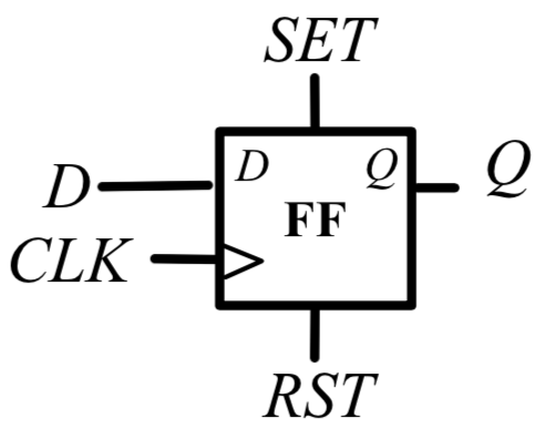
Fig. 59 An example of classical Flip-Flop.
The code describing this FF is:
<circuit_model type="ff" name="dff" prefix="dff" verilog_netlist="ff.v" spice_netlist="ff.sp">
  <port type="input" prefix="D" lib_name="D" size="1"/>
  <port type="input" prefix="Set" lib_name="S" size="1" is_global="true"/>
  <port type="input" prefix="Reset" lib_name="R" size="1" is_global="true"/>
  <port type="output" prefix="Q" lib_name="Q" size="1"/>
  <port type="clock" prefix="clk" lib_name="CK" size="1" is_global="true"/>
</circuit_model>
- This example shows:
A regular flip-flop which is defined in a Verilog netlist
ff.vand a SPICE netlistff.spThe flip-flop has
setandresetfunctionalitiesThe flip-flop port names defined differently in standard cell library and VPR architecture. The
lib_namecapture the port name defined in standard cells, whileprefixcapture the port name defined inpb_typeof VPR architecture file
Multi-mode Flip-Flop
Fig. 60 illustrates an example of a flip-flop which can be operate in different modes.

Fig. 60 An example of a flip-flop which can be operate in different modes
The code describing this FF is:
<circuit_model type="ff" name="frac_ff" prefix="frac_ff" verilog_netlist="frac_ff.v" spice_netlist="frac_ff.sp">
  <port type="input" prefix="D" lib_name="D" size="1"/>
  <port type="input" prefix="Reset" lib_name="RST_OP" size="1" is_global="true"/>
  <port type="output" prefix="Q" lib_name="Q" size="1"/>
  <port type="clock" prefix="clock" lib_name="CLK" size="1" is_global="true"/>
  <port type="sram" prefix="MODE" lib_name="MODE" size="1" mode_select="true" circuit_model_name="CCFF" default_value="0"/>
</circuit_model>
- This example shows:
A multi-mode flip-flop which is defined in a Verilog netlist
frac_ff.vand a SPICE netlistfrac_ff.spThe flip-flop has a
resetpin which can be either active-low or active-high, depending on the mode selection pinMODE.The mode-selection bit will be generated by a configurable memory outside the flip-flop, which will be implemented by a circuit model
CCFFdefined by users (see an example in Regular Configuration-chain Flip-flop).The flip-flop port names defined differently in standard cell library and VPR architecture. The
lib_namecapture the port name defined in standard cells, whileprefixcapture the port name defined inpb_typeof VPR architecture file
Configuration Chain Flip-Flop
Note
OpenFPGA does not auto-generate any netlist for configuration chain flip-flops. Users should define the HDL modeling in external netlists and ensure consistency to physical designs.
Template
<circuit_model type="ccff" name="<string>" prefix="<string>" spice_netlist="<string>" verilog_netlist="<string>"/>
  <design_technology type="cmos"/>
  <input_buffer exist="<string>" circuit_model_name="<string>"/>
  <output_buffer exist="<string>" circuit_model_name="<string>"/>
  <port type="input" prefix="<string>" size="<int>"/>
  <port type="output" prefix="<string>" size="<int>"/>
  <port type="clock" prefix="<string>" size="<int>"/>
</circuit_model>
Note
The circuit designs of configurable memory elements are highly dependent on the technology node and well optimized by engineers. Therefore, FPGA-Verilog/SPICE requires users to provide their customized FF Verilog/SPICE/Verilog netlists. A sample Verilog/SPICE netlist of FF can be found in the directory SpiceNetlists in the released package.
The information of input and output buffer should be clearly specified according to the customized SPICE netlist! The existence of input/output buffers will influence the decision in creating SPICE testbenches, which may leads to larger errors in power analysis.
Note
FPGA-Verilog/SPICE currently support only one clock domain for any configuration protocols in the FPGA. Therefore there should be only one clock port to be defined and the size of the clock port should be 1.
Note
A flip-flop should at least have three types of ports, input, output and clock.
Note
If the user provides a customized Verilog/SPICE netlist, the bandwidth of ports should be defined to the same as the Verilog/SPICE netlist.
Note
In a valid FPGA architecture, users should provide at least either a ccff or sram circuit model, so that the configurations can loaded to core logic.
Regular Configuration-chain Flip-flop
Fig. 61 illustrates an example of standard flip-flops used to build a configuration chain.

Fig. 61 An example of a Flip-Flop organized in a chain.
The code describing this FF is:
<circuit_model type="ccff" name="ccff" prefix="ccff" verilog_netlist="ccff.v" spice_netlist="ccff.sp">
  <port type="input" prefix="D" size="1"/>
  <port type="output" prefix="Q" size="1"/>
  <port type="output" prefix="QN" size="1"/>
  <port type="clock" prefix="CK" size="1" is_global="true" is_prog="true" is_clock="true"/>
</circuit_model>
- This example shows:
A configuration-chain flip-flop which is defined in a Verilog netlist
ccff.vand a SPICE netlistccff.spThe flip-flop has a global clock port,
CK, which will be wired a global programming clock
Note
- The output ports of the configuration flip-flop must follow a fixed sequence in definition:
The first output port MUST be the data output port, e.g.,
Q.The second output port MUST be the inverted data output port, e.g.,
QN.
Configuration-chain Flip-flop with Configure Enable Signals
Configuration chain could be built with flip-flops with outputs that are enabled by specific signals. Consider the example in Fig. 62, the flip-flop has
a configure enable signal
CFG_ENto release the data outputQandQNa pair of data outputs
QandQNwhich are controlled by the configure enable signalCFG_ENa regular data output
SCAN_Qwhich outputs registered data

Fig. 62 An example of a Flip-Flop with config enable feature organized in a chain.
The code describing this FF is:
<circuit_model type="ccff" name="ccff" prefix="ccff" verilog_netlist="ccff.v" spice_netlist="ccff.sp">
  <port type="input" prefix="CFG_EN" size="1" is_global="true" is_config_enable="true"/>
  <port type="input" prefix="D" size="1"/>
  <port type="output" prefix="SCAN_Q" size="1"/>
  <port type="output" prefix="QN" size="1"/>
  <port type="output" prefix="Q" size="1"/>
  <port type="clock" prefix="CK" size="1" is_global="true" is_prog="true" is_clock="true"/>
</circuit_model>
Note
- The output ports of the configuration flip-flop must follow a fixed sequence in definition:
The first output port MUST be the regular data output port, e.g.,
SCAN_Q.The second output port MUST be the inverted data output port which is activated by the configure enable signal, e.g.,
QN.The second output port MUST be the data output port which is activated by the configure enable signal, e.g.,
Q.
Configuration-chain Flip-flop with Scan Input
Configuration chain could be built with flip-flops with a scan chain input . Consider the example in Fig. 63, the flip-flop has
an additional input
SIto enable scan-chain capabailitya configure enable signal
CFG_ENto release the data outputQandQNa pair of data outputs
QandQNwhich are controlled by the configure enable signalCFG_ENa regular data output
SCAN_Qwhich outputs registered data

Fig. 63 An example of a Flip-Flop with scan input organized in a chain.
The code describing this FF is:
<circuit_model type="ccff" name="ccff" prefix="ccff" verilog_netlist="ccff.v" spice_netlist="ccff.sp">
  <port type="input" prefix="CFG_EN" size="1" is_global="true" is_config_enable="true"/>
  <port type="input" prefix="D" size="1"/>
  <port type="input" prefix="SI" size="1"/>
  <port type="output" prefix="SCAN_Q" size="1"/>
  <port type="output" prefix="QN" size="1"/>
  <port type="output" prefix="Q" size="1"/>
  <port type="clock" prefix="CK" size="1" is_global="true" is_prog="true" is_clock="true"/>
</circuit_model>
Note
- The input ports of the configuration flip-flop must follow a fixed sequence in definition:
The first input port MUST be the regular data input port, e.g.,
D.The second input port MUST be the scan input port, e.g.,
SI.
Hard Logics
Note
OpenFPGA does not auto-generate any netlist for the hard logics. Users should define the HDL modeling in external netlists and ensure consistency to physical designs.
Template
<circuit_model type="hardlogic" name="<string>" prefix="<string>" verilog_netlist="<string>" spice_netlist="<string>"/>
  <design_technology type="cmos"/>
  <input_buffer exist="<string>" circuit_model_name="<string>"/>
  <output_buffer exist="<string>" circuit_model_name="<string>"/>
  <port type="input" prefix="<string>" size="<int>"/>
  <port type="output" prefix="<string>" size="<int>"/>
</circuit_model>
Note
Hard logics are defined for non-configurable resources in FPGA architectures, such as adders, multipliers and RAM blocks. Their circuit designs are highly dependent on the technology node and well optimized by engineers. As more functional units are included in FPGA architecture, it is impossible to auto-generate these functional units. Therefore, FPGA-Verilog/SPICE requires users to provide their customized Verilog/SPICE netlists.
Note
Examples can be found in hard_logic_example_link
Note
The information of input and output buffer should be clearly specified according to the customized Verilog/SPICE netlist! The existence of input/output buffers will influence the decision in creating SPICE testbenches, which may leads to larger errors in power analysis.
Full Adder

Fig. 64 An example of a 1-bit full adder.
The code describing the 1-bit full adder is:
<circuit_model type="hard_logic" name="adder" prefix="adder" spice_netlist="adder.sp" verilog_netlist="adder.v">
  <design_technology type="cmos"/>
  <input_buffer exist="true" circuit_model_name="inv1x"/>
  <output_buffer exist="true" circuit_model_name="inv1x"/>
  <port type="input" prefix="a" size="1"/>
  <port type="input" prefix="b" size="1"/>
  <port type="input" prefix="cin" size="1"/>
  <port type="output" prefix="cout" size="1"/>
  <port type="output" prefix="sumout" size="1"/>
</circuit_model>
- This example shows:
A 1-bit full adder which is defined in a Verilog netlist
adder.vand a SPICE netlistadder.spThe adder has three 1-bit inputs, i.e.,
a,bandcin, and two 2-bit outputs, i.e.,cout,sumout.
Multiplier

Fig. 65 An example of a 8-bit multiplier.
The code describing the multiplier is:
<circuit_model type="hard_logic" name="mult8x8" prefix="mult8x8" spice_netlist="dsp.sp" verilog_netlist="dsp.v">
  <design_technology type="cmos"/>
  <input_buffer exist="true" circuit_model_name="inv1x"/>
  <output_buffer exist="true" circuit_model_name="inv1x"/>
  <port type="input" prefix="a" size="8"/>
  <port type="input" prefix="b" size="8"/>
  <port type="output" prefix="out" size="16"/>
</circuit_model>
- This example shows:
A 8-bit multiplier which is defined in a Verilog netlist
dsp.vand a SPICE netlistdsp.sp
Multi-mode Multiplier

Fig. 66 An example of a 8-bit multiplier which can operating in two modes: (1) dual 4-bit multipliers; and (2) 8-bit multiplier
The code describing the multiplier is:
<circuit_model type="hard_logic" name="frac_mult8x8" prefix="frac_mult8x8" spice_netlist="dsp.sp" verilog_netlist="dsp.v">
  <design_technology type="cmos"/>
  <input_buffer exist="true" circuit_model_name="inv1x"/>
  <output_buffer exist="true" circuit_model_name="inv1x"/>
  <port type="input" prefix="a" size="8"/>
  <port type="input" prefix="b" size="8"/>
  <port type="output" prefix="out" size="16"/>
  <port type="sram" prefix="mode" size="1" mode_select="true" circuit_model_name="CCFF" default_value="0"/>
</circuit_model>
- This example shows:
A multi-mode 8-bit multiplier which is defined in a Verilog netlist
dsp.vand a SPICE netlistdsp.spThe multi-mode multiplier can operating in two modes: (1) dual 4-bit multipliers; and (2) 8-bit multiplier
The mode-selection bit will be generated by a configurable memory outside the flip-flop, which will be implemented by a circuit model
CCFFdefined by users (see an example in Regular Configuration-chain Flip-flop).
Dual Port Block RAM

Fig. 67 An example of a dual port block RAM with 128 addresses and 8-bit data width.
The code describing this block RAM is:
<circuit_model type="hard_logic" name="dpram_128x8" prefix="dpram_128x8" spice_netlist="dpram.sp" verilog_netlist="dpram.v">
  <design_technology type="cmos"/>
  <input_buffer exist="true" circuit_model_name="inv1x"/>
  <output_buffer exist="true" circuit_model_name="inv1x"/>
  <port type="input" prefix="waddr" size="7"/>
  <port type="input" prefix="raddr" size="7"/>
  <port type="input" prefix="data_in" size="8"/>
  <port type="input" prefix="wen" size="1"/>
  <port type="input" prefix="ren" size="1"/>
  <port type="output" prefix="data_out" size="8"/>
  <port type="clock" prefix="clock" size="1" is_global="true" default_val="0"/>
</circuit_model>
- This example shows:
A 128x8 dual port RAM which is defined in a Verilog netlist
dpram.vand a SPICE netlistdpram.spThe clock port of the RAM is controlled by a global signal (see details about global signal definition in Physical Tile Annotation).
Multi-mode Dual Port Block RAM

Fig. 68 An example of a dual port block RAM which can operate in two modes: 128x8 and 256x4.
The code describing this block RAM is:
<circuit_model type="hard_logic" name="frac_dpram_128x8" prefix="frac_dpram_128x8" spice_netlist="frac_dpram.sp" verilog_netlist="frac_dpram.v">
  <design_technology type="cmos"/>
  <input_buffer exist="true" circuit_model_name="inv1x"/>
  <output_buffer exist="true" circuit_model_name="inv1x"/>
  <port type="input" prefix="waddr" size="8"/>
  <port type="input" prefix="raddr" size="8"/>
  <port type="input" prefix="data_in" size="8"/>
  <port type="input" prefix="wen" size="1"/>
  <port type="input" prefix="ren" size="1"/>
  <port type="output" prefix="data_out" size="8"/>
  <port type="clock" prefix="clock" size="1" is_global="true" default_val="0"/>
  <port type="sram" prefix="mode" size="1" mode_select="true" circuit_model_name="CCFF" default_value="0"/>
</circuit_model>
- This example shows:
A fracturable dual port RAM which is defined in a Verilog netlist
frac_dpram.vand a SPICE netlistfrac_dpram.spThe dual port RAM can operate in two modes: (1) 128 addresses with 8-bit data width; (2) 256 addresses with 4-bit data width
The clock port of the RAM is controlled by a global signal (see details about global signal definition in Physical Tile Annotation).
The mode-selection bit will be generated by a configurable memory outside the flip-flop, which will be implemented by a circuit model
CCFFdefined by users (see an example in Regular Configuration-chain Flip-flop).
Routing Wire Segments
FPGA architecture requires two type of wire segments:
wire, which targets the local wires inside the logic blocks. The wire has one input and one output, directly connecting the output of a driver and the input of the downstream unit, respectively
chan_wire, especially targeting the channel wires. The channel wires have one input and two outputs, one of which is connected to the inputs of Connection Boxes while the other is connected to the inputs of Switch Boxes. Two outputs are created because from the view of layout, the inputs of Connection Boxes are typically connected to the middle point of channel wires, which has less parasitic resistances and capacitances than connected to the ending point.
Template
<circuit_model type="wire|cham_wire" name="<string>" prefix="<string>" spice_netlist="<string>" verilog_netlist="<string>"/>
  <design_technology type="cmos"/>
  <input_buffer exist="<string>" circuit_model_name="<string>"/>
  <output_buffer exist="<string>" circuit_model_name="<string>"/>
  <port type="input" prefix="<string>" size="<int>"/>
  <port type="output" prefix="<string>" size="<int>"/>
  <wire_param model_type="<string>" R="<float>" C="<float>" num_level="<int>"/>
</circuit_model>
Note
FPGA-Verilog/SPICE can auto-generate the Verilog/SPICE model for wires while also allows users to provide their customized Verilog/SPICE netlists.
Note
The information of input and output buffer should be clearly specified according to the customized netlist! The existence of input/output buffers will influence the decision in creating testbenches, which may leads to larger errors in power analysis.
- <wire_param model_type="<string>" R="<float>" C="<float>" num_level="<int>"/>
model_type="pi|T"Specify the type of RC models for this wire segement. Currently, OpenFPGA supports the \(\pi\)-type and T-type multi-level RC models.R="<float>"Specify the total resistance of the wireC="<float>"Specify the total capacitance of the wire.num_level="<int>"Specify the number of levels of the RC wire model.
Note
wire parameters are essential for FPGA-SPICE to accurately model wire parasitics
Routing Track Wire Example
Fig. 69 depicts the modeling for a length-2 channel wire.
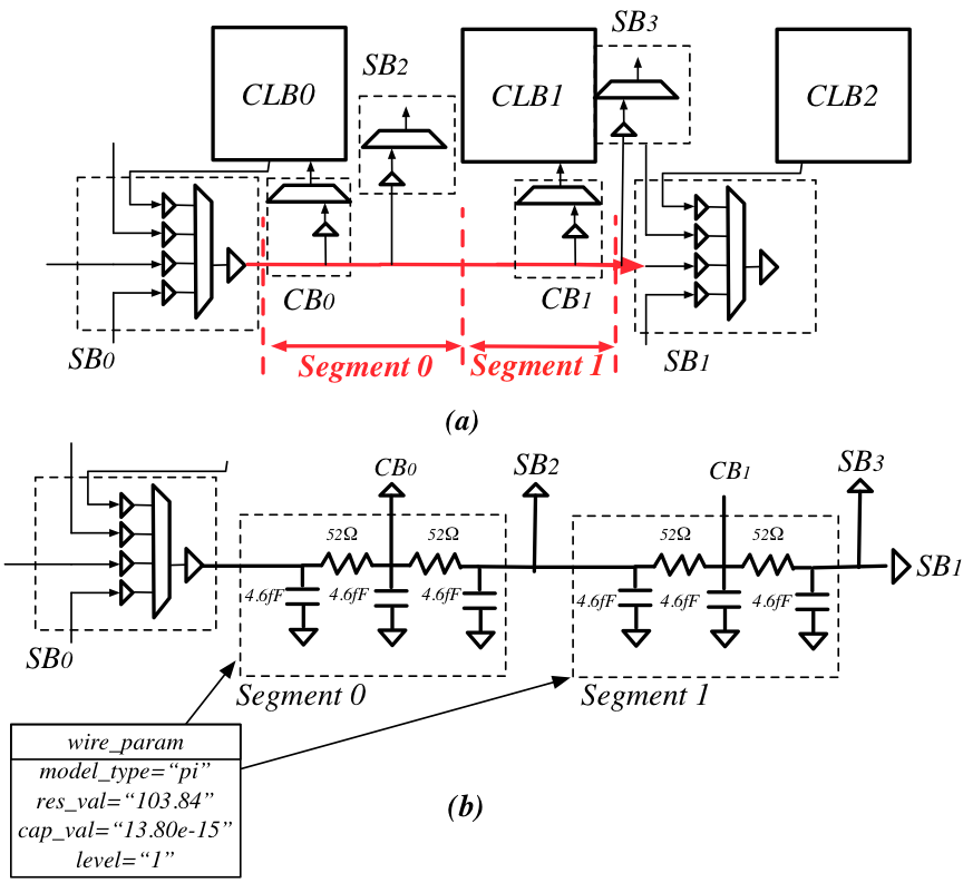
Fig. 69 An example of a length-2 channel wire modeling
The code describing this wire is:
<circuit_model type="chan_wire" name="segment0" prefix="chan_wire"/>
  <design_technology type="cmos"/>
  <port type="input" prefix="mux_out" size="1"/>
  <port type="output" prefix="cb_sb" size="1"/>
  <wire_param model_type="pi" res_val="103.84" cap_val="13.80e-15" level="1"/>
</circuit_model>
- This example shows
A routing track wire has 1 input and output
The routing wire will be modelled as a 1-level \(\pi\)-type RC wire model with a total resistance of \(103.84\Omega\) and a total capacitance of \(13.89fF\)
I/O pads
Note
OpenFPGA does not auto-generate any netlist for I/O cells. Users should define the HDL modeling in external netlists and ensure consistency to physical designs.
Template
<circuit_model type="iopad" name="<string>" prefix="<string>" spice_netlist="<string>" verilog_netlist="<string>"/>
  <design_technology type="cmos"/>
  <input_buffer exist="<string>" circuit_model_name="<string>"/>
  <output_buffer exist="<string>" circuit_model_name="<string>"/>
  <port type="input" prefix="<string>" size="<int>"/>
  <port type="output" prefix="<string>" size="<int>"/>
  <port type="sram" prefix="<string>" size="<int>" mode_select="<bool>" circuit_model_name="<string>" default_val="<int>"/>
</circuit_model>
Note
The circuit designs of I/O pads are highly dependent on the technology node and well optimized by engineers. Therefore, FPGA-Verilog/SPICE requires users to provide their customized Verilog/SPICE/Verilog netlists. A sample Verilog/SPICE netlist of an I/O pad can be found in the directory SpiceNetlists in the released package.
Note
The information of input and output buffer should be clearly specified according to the customized netlist! The existence of input/output buffers will influence the decision in creating testbenches, which may leads to larger errors in power analysis.
General Purpose I/O
Fig. 70 depicts a general purpose I/O pad.
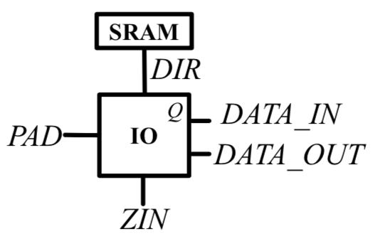
Fig. 70 An example of an IO-Pad
The code describing this I/O-Pad is:
<circuit_model type="iopad" name="iopad" prefix="iopad" spice_netlist="io.sp" verilog_netlist="io.v">
  <design_technology type="cmos"/>
  <input_buffer exist="true" circuit_model_name="INVTX1"/>
  <output_buffer exist="true" circuit_model_name="INVTX1"/>
  <pass_gate_logic circuit_model_name="TGATE"/>
  <port type="inout" prefix="pad" size="1" is_global="true" is_io="true" is_data_io="true"/>
  <port type="sram" prefix="en" size="1" mode_select="true" circuit_model_name="ccff" default_val="1"/>
  <port type="input" prefix="outpad" size="1"/>
  <port type="output" prefix="inpad" size="1"/>
</circuit_model>
- This example shows
A general purpose I/O cell defined in Verilog netlist
io.spand SPICE netlistio.spThe I/O cell has an
inoutport as the bi-directional portThe directionality of I/O can be controlled by a configuration-chain flip-flop defined in circuit model
ccffIf unused, the I/O cell will be configured to
1