Read a Memory Initialization File in the OpenFPGA MIF format (see below), parse it, and append the resulting segment(s) to in-memory storage. May be run multiple times; each successful read appends more segments. Intended before link_openfpga_arch when the flow uses MIF-based BRAM initialization.
Format (summary)
Line comments: #... or //... (// directives are described next).
Optional tile coordinates: //X<int>, //Y<int> (# may follow on the same line).
A new RAM block section starts at //RAM_ID<int>; data lines before the first //RAM_ID belong to the placement-oriented block (X/Y); following lines belong to the RAM_ID block.
Data lines: <hex_address><hex_data> (e.g. 0x20000x0000000a), exactly two tokens per line.
Write the processed in-memory MIF data to one file in the OpenFPGA MIF format. Requires that read_mif has completed successfully at least once before this command (shell dependency).
Build the routing resource graph based on an defined programmable clock network, and append it to the existing routing resource graph built by VPR.
Use command openfpga_setup_command_read_openfpga_clock_arch` to load the clock network.
Route clock signals on the built routing resource graph which contains a programmable clock network.
Clock signals will be auto-detected and routed based on pin constraints which are provided by users.
Specify the Pin Constraints File (PCF) when the clock network contains multiple clock pins. For example, -pin_constraints_filepin_constraints.xml. Strongly recommend for multi-clock network. See detailed file format about Pin Constraints File (.xml).
Note
If there is a global net, e.g., clk or reset, which will be driven by an internal resource, it should also be defined in the PCF file.
Specify the signal activity file. For example, --activity_filecounter.act.
This is required when users wants OpenFPGA to automatically find the number of clocks in simulations. See details at Simulation settings.
Sort the OPIN edges in General Switch Blocks (GSBs). Ensure the OPINs come first before channel edges, this is performed after executing –sort_gsb_chan_node_in_edges option.
Allow dangling output ports exist without driving any routing tracks in General Switch Blocks (GSBs). By default, it is disabled to keep netlist clean and maximize the efficiency in uniquifying routing blocks. Enable it to ensure support on legacy devices.
Write the internal structure of General Switch Blocks (GSBs) across a FPGA fabric, including the interconnection between the nodes and node-level details, to XML files. Please refer General Switch Blocks (GSB) for details about the file format.
Exclude routing resource graph information from output files, e.g., node id as well as other attributes. This is useful to check the connection inside GSBs purely.
Specify the name of GSB to be outputted. Users can specify multiple GSBs by using a splitter ,.
When specified, only the GSBs whose names match the list will be outputted to files.
If not specified, all the GSBs will be outputted.
Note
When option --unique is enable, the given name of GSBs should match the unique modules!
Check and correct any naming conflicts in the BLIF netlist
This is strongly recommended. Otherwise, the outputted Verilog netlists may not be compiled successfully.
Warning
This command may be deprecated in future when it is merged to VPR upstream
Apply fix-up to clustering nets based on routing results
Note
Suggest to skip the similar fix-up applied by VPR through options --skip_sync_clustering_and_routing_resultson when calling vpr in openfpga shell.
Warning
This feature has been integrated into VPR to provide accurate timing analysis results at post-routing stage. However, this command provides a light fix-up (not as thorough as the one in VPR) but bring more flexibility in support some architecture without local routing. Suggest to enable it when your architecture does not have local routing for Look-Up Tables (LUTs) but you want to enable logic equivalent for input pins of LUTs
If specified, any global net including clock, reset etc, will be mapped to a best-fit Most Significant Bit (MSB) of input ports of programmable blocks. If not specified, a best-fit Least Significant Bit (LSB) will be the default choice. For example, when --clock_modelingideal is selected when running VPR, global nets will not be routed and their pin mapping on programmable blocks may be revoked by other nets due to optimization. Therefore, this command will restore the pin mapping for the global nets and pick a spare pin on programmable blocks. This option is to set a preference when mapping the global nets to spare pins.
Enable compression on routing architecture modules. Strongly recommend this as it will minimize the number of routing modules to be outputted. It can reduce the netlist size significantly.
Group fine-grained programmable blocks, connection blocks and switch blocks into tiles. Once enabled, tiles will be added to the top-level module. Otherwise, the top-level module consists of programmable blocks, connection blocks and switch blocks. The tile style can be customized through a file. See details in Tile Organization (.xml). When enabled, the Verilog netlists will contain additional netlists that model tiles (see details in Tiles).
Warning
This option does not support --duplicate_grid_pin!
Warning
This option requires --compress_routing to be enabled!
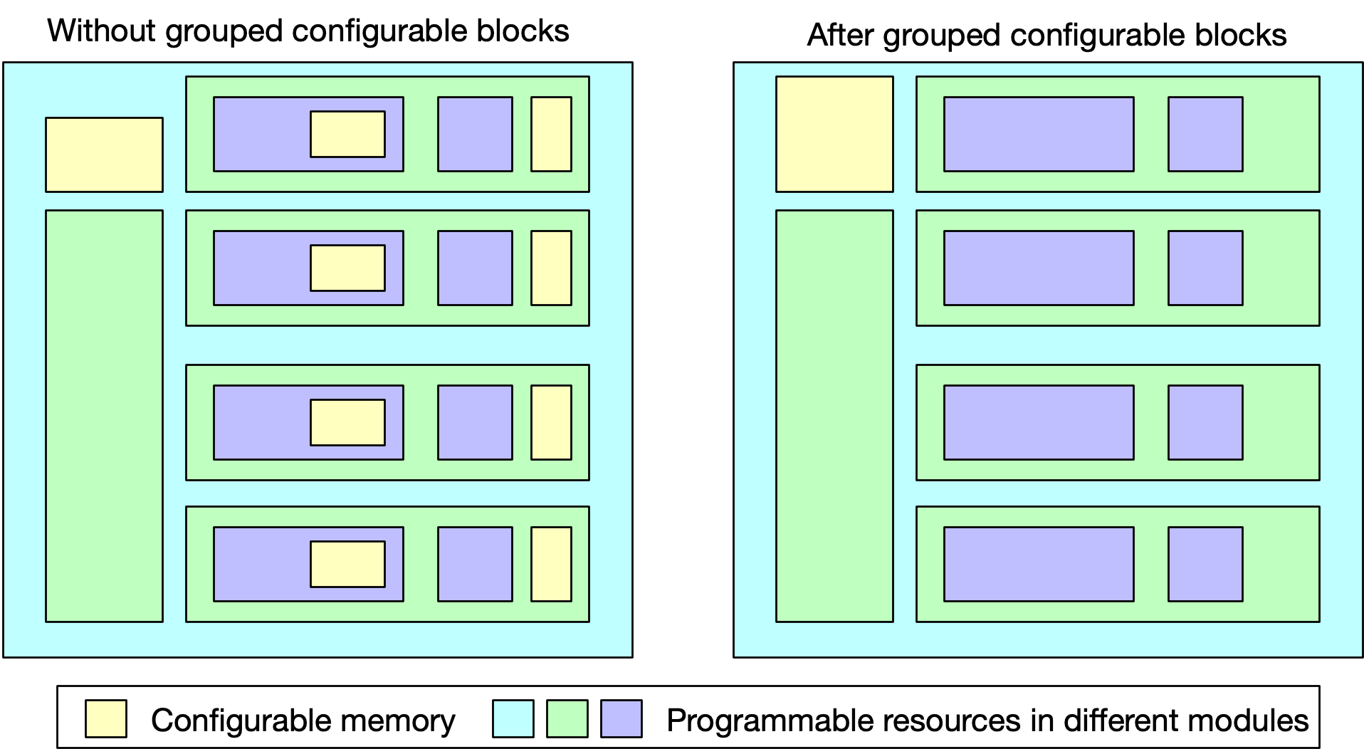
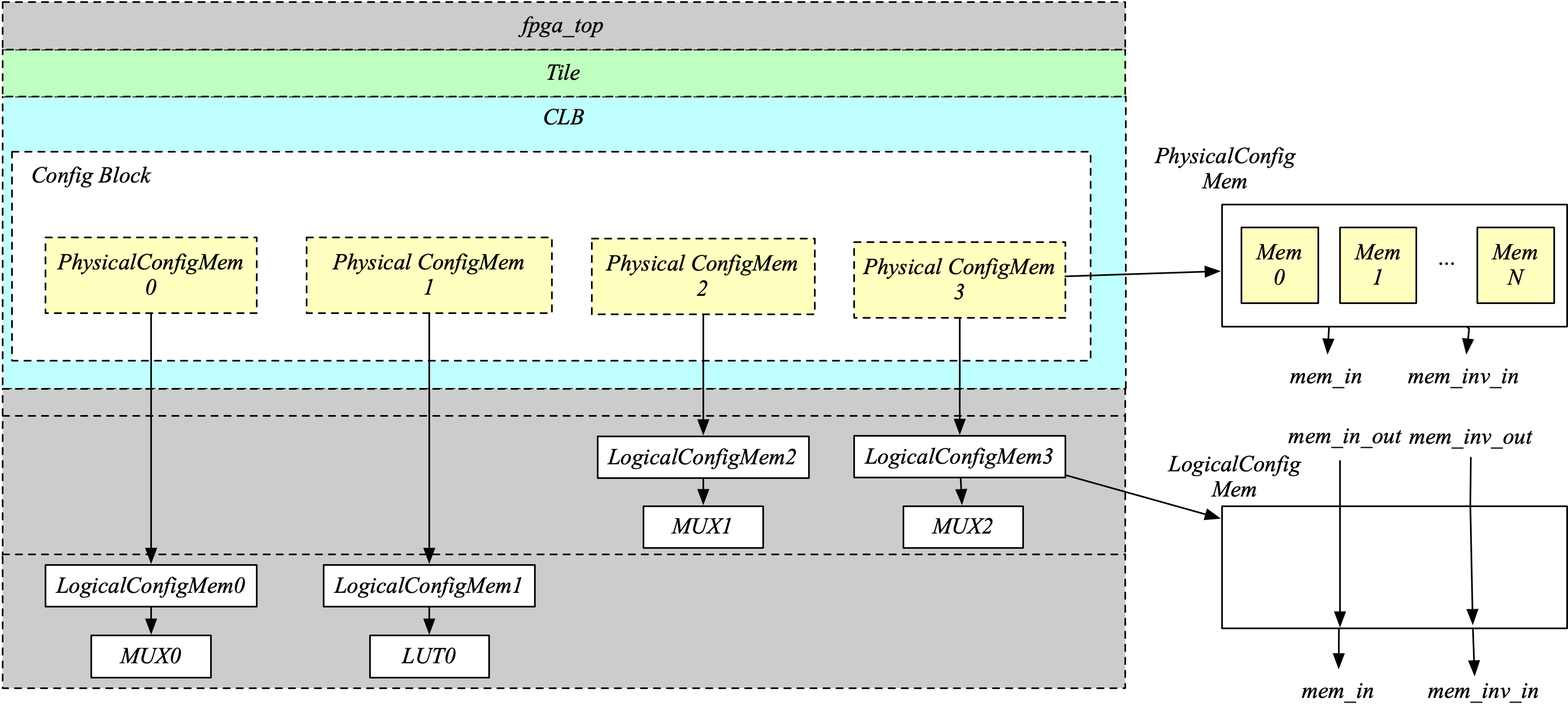
Group configuration memory blocks under each CLB/SB/CB etc. into a centralized configuration memory blocks, as depicted in Fig. 75. When disabled, the configuration memory blocks are placed in a distributed way under CLB/SB/CB etc. For example, each programming resource, e.g., LUT, has a dedicated configuration memory block, being placed in the same module. When enabled, as illustrated in Fig. 76, the physical memory block locates under a CLB, driving a number of logical memory blocks which are close to the programmable resources. The logical memory blocks contain only pass-through wires which can be optimized out during physical design phase.
Adding this option will combine connection block and switch block into a single module (Currently named as SB_*__*_). The IPIN and OPIN of the grid makes connection to SB directly instead of going through a connection block. This is helpful, when IPIN is connected to CHANX and CHANY together, or to the both side of the Switchboxes.
Use index in module names, e.g., cbx_2_. This is applied to routing modules, as well as tile modules when option --group_tile is enabled. If disabled, the module name consist of coordinates, e.g., cbx_1__2_.
Create only frame views of the module graph. When enabled, top-level module will not include any nets. This option is made for save runtime and memory.
Warning
Recommend to turn the option on when bitstream generation is the only purpose of the flow. Do not use it when you need generate netlists!
Output current fabric key to an XML file. For example, write_fabric_key--filefpga_2x2.xml See details in Fabric Key (.xml).
Note
This command can output module-level keys while the --write_fabric_key option in command build_fabric does NOT support! Strongly recommend to use this command to obtain fabric key.
Add a wrapper module fpga_core as an intermediate layer to FPGA fabric. After this command, the existing module fpga_top will remain the top-level module while there is a new module fpga_core under it. Under fpga_core, there will be the detailed building blocks.
This is optional. Specify the I/O naming rules when connecting I/Os of fpga_core module to the top-level module fpga_top. If not defined, the fpga_top will be the same as fpga_core w.r.t. ports. See details about the file format of I/O naming rules in Fabric I/O Naming (.xml).
This is optional. Specify the instance name to be used when instanciate the fpga_core module under the top-level module fpga_top. If not defined, by default it is fpga_core_inst.
Create only frame views of the module graph. When enabled, top-level module will not include any nets. This option is made for save runtime and memory.
Warning
Recommend to turn the option on when bitstream generation is the only purpose of the flow. Do not use it when you need generate netlists!
Specify at which depth of the fabric module graph should the writer stop outputting. The root module start from depth 0. For example, if you want a two-level hierarchy, you should specify depth as 1.
Specify the root module name(s) which should be considered. By default, it is fpga_top. Note that regular expression is supported. For example, grid_* will output all the modules with a prefix of grid_
Specify the filter which allows user to select modules to appear under each root module tree. By default, it is *. Regular expression is supported. For example, *mux* will output all the modules which contains mux. In the other words, the filter defines a white list.
Specify the naming convention for ports in pin table files from which pin direction can be inferred. Can be [explicit``|``quicklogic]. When explicit is selected, pin direction is inferred based on the explicit definition in a column of pin table file, e.g., GPIO direction (see details in Pin Table File (.csv)). When quicklogic is selected, pin direction is inferred by port name: a port whose postfix is _A2F is an input, while a port whose postfix is _A2F is an output. By default, it is explicit.
Reduce error to warning while reading commands in pcf file
Warning
Exercise extreme caution when adding this option – be sure you completely understand why the issue is being flagged, and why it is OK to treat as a warning instead of an error.
Specify the naming convention for ports in pin table files from which pin direction can be inferred. Can be [explicit``|``quicklogic]. When explicit is selected, pin direction is inferred based on the explicit definition in a column of pin table file, e.g., GPIO direction (see details in Pin Table File (.csv)). When quicklogic is selected, pin direction is inferred by port name: a port whose postfix is _A2F is an input, while a port whose postfix is _A2F is an output. By default, it is explicit.
Specify the path to the input sdc file (.sdc). The generated SDC content will be appended to this file. If not specified, a new file will be created and the SDC will be written to the output_sdc path
Reduce error to warning while reading commands in pcf file
Warning
Exercise extreme caution when adding this option – be sure you completely understand why the issue is being flagged, and why it is OK to treat as a warning instead of an error.
Specify the name of modules to be considered. Support regular expression, e.g., tile*. When provided, only pins of selected modules will be outputted. By default, a wildcard * is considered, which means all the modules will be considered.
Specify the naming convention for ports in pin table files from which pin direction can be inferred. Can be [explicit``|``quicklogic]. When explicit is selected, pin direction is inferred based on the explicit definition in a column of pin table file, e.g., GPIO direction (see details in Pin Table File (.csv)). When quicklogic is selected, pin direction is inferred by port name: a port whose postfix is _A2F is an input, while a port whose postfix is _A2F is an output. By default, it is explicit